
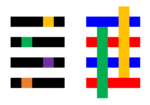
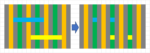
There has been much interest in Huawei’s and SMIC’s plans for 5nm production in the near future. Since there is no use of EUV in China, immersion DUV lithography (with a 76 nm pitch resolution) is expected to be used along with pitch quartering to achieve pitches in the 20-30 nm range expected for the 5nm and 3nm nodes [1].… Read More

Author: Fred Chen
Huawei’s and SMIC’s Requirement for 5nm Production: Improving Multipatterning Productivity
Measuring Local EUV Resist Blur with Machine Learning
Resist blur remains a topic that is relatively unexplored in lithography. Blur has the effect of reducing the difference between the maximum and minimum doses in the local region containing the feature. Blur is particularly important for EUV lithography since EUV lithography is prone to stochastic fluctuations and also driven… Read More
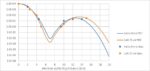
Pinning Down an EUV Resist’s Resolution vs. Throughput
The majority of EUV production is on 5nm and 3nm node, implemented by late 2022. Metal oxide resists have not been brought into volume production yet [1,2], meaning that only organic chemically amplified resists (CARs) have been used instead until now. These resists have a typical absorption coefficient of 5/um [3,4], which means
Application-Specific Lithography: Avoiding Stochastic Defects and Image Imbalance in 6-Track Cells
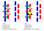
The discussion of any particular lithographic application often refers to imaging a single pitch, e.g., 30 nm pitch for a 5nm-family track metal scenario. However, it is always necessary to confirm the selected patterning techniques on the actual use case. The 7nm, 5nm, or 3nm 6-track cell has four minimum pitch tracks, flanked… Read More
Non-EUV Exposures in EUV Lithography Systems Provide the Floor for Stochastic Defects in EUV Lithography
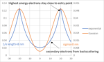
EUV lithography is a complicated process with many factors affecting the production of the final image. The EUV light itself doesn’t directly generate the images, but acts through secondary electrons which are released as a result of ionization by incoming EUV photons. Consequently, we need to be aware of the fluctuations… Read More
Application-Specific Lithography: Sense Amplifier and Sub-Wordline Driver Metal Patterning in DRAM
On a DRAM chip, the patterning of features outside the cell array can be just as challenging as those within the array itself. While the array contains features which are the most densely packed, at least they are regularly arranged. On the other hand, outside the array, the regularity is lost, but the in the most difficult cases, … Read More
BEOL Mask Reduction Using Spacer-Defined Vias and Cuts
In recent advanced nodes, via and cut patterning have constituted a larger and larger portion of the overall BEOL mask count. The advent of SALELE [1,2] caused mask count to increase for EUV as well, resulting in costs no longer being competitive with DUV down to 3nm [3]. Further development by TEL [4] has shown the possibility for… Read More
Predicting Stochastic Defectivity from Intel’s EUV Resist Electron Scattering Model
The release and scattering of photoelectrons and secondary electrons in EUV resists has often been glossed over in most studies in EUV lithography, despite being a fundamental factor in the image formation. Fortunately, Intel has provided us with a laboriously simulated electron release and scattering model, using the GEANT4… Read More
The Significance of Point Spread Functions with Stochastic Behavior in Electron-Beam Lithography
Electron beam lithography is commercially used to directly write submicron patterns onto advanced node masks. With the advent of EUV masks and nanometer-scale NIL (nanoimprint lithography), multi-beam writers are now being used, compensating the ultralow throughput of a single high-resolution electron beam with the use… Read More
Extension of DUV Multipatterning Toward 3nm
China’s recent achievement of a 7nm-class foundry node using only DUV lithography [1] raises the question of how far DUV lithography can be extended by multipatterning. A recent publication at CSTIC 2023 indicates that Chinese groups are currently looking at extension of DUV-based multipatterning to 5nm, going so far… Read More


Intel, Musk, and the Tweet That Launched a 1000 Ships on a Becalmed Sea