You are currently viewing SemiWiki as a guest which gives you limited access to the site. To view blog comments and experience other SemiWiki features you must be a registered member. Registration is fast, simple, and absolutely free so please,
join our community today!
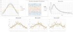
Electron blur, stochastics, and now polarization, are all becoming stronger influences in EUV lithography as pitch continues to shrink
As EUV lithography continues to evolve, targeting smaller and smaller pitches, new physical limitations continue to emerge as formidable obstacles. While stochastic effects have long been… Read More
Two approaches compared
With half-pitch approaching 10 nm, EUV patterning is heavily impacted by stochastic effects, which are aggravated from reduced image contrast from electron blur [1]. A two-mask (“LELE”: Litho-Etch-Litho-Etch) approach was proposed to pattern core features for self-aligned double patterning (SADP)… Read More
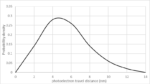
Peak probability at zero distance actually makes no sense
In lithography, it is often stated that the best resolution that can be achieved depends on wavelength and numerical aperture (NA), but this actually only applies to the so-called “aerial” image. When the image is actually formed in the resist layer, it also depends on an… Read More
Whether EUV or DUV doesn’t matter at 20 nm pitch
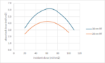
The International Roadmap for Devices and Systems, 2022 Edition, indicates that the “2nm” node due in 2025 (this year) has a minimum (metal) half-pitch of 10 nm [1]. This is, in fact, less than the resolution of a current state-of-the-art EUV system, with a numerical aperture… Read More
The occurrences of notorious stochastic defects in EUV lithography have resulted in CD or corresponding dose windows with the lower and higher bounds being characterized as “cliffs” [1-3], since the defect density increases exponentially when approaching these bounds. The defects at lower doses have been attributed to the… Read More
Conventionally, the resolution limit of a lithography system with wavelength l and numerical aperture NA is given by half-pitch = 0.25 wavelength/NA. With the use of EUV lithography, however, electron blur needs to be added [1]. The impact of this blur is to reduce the contrast [2]. Blur reduces the modulation amplitude by a factor… Read More
Previously, I had indicated how detrimental stochastic effects at pitches below 50 nm should lead to reconsidering the practical resolution limit for EUV lithography [1]. This is no exaggeration, as stochastic effects have been observed for 24 nm half-pitch several years ago [2,3]. This then leads to the question of whether … Read More
Pupil fill tradeoff again
EUV lithography continues to be plagued by its stochastic nature.
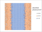
This stochastic nature is most clearly portrayed by the random fluctuation of the absorbed photon number at a given location. For example, consider an absorbed dose of 10 mJ/cm2 amounts to 6.8 photons of energy 92 eV absorbed in a square … Read More
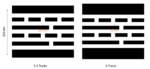
At IEDM 2019, TSMC revealed two versions of 5nm standard cell layouts: a 5.5-track DUV-patterned version and a 6-track EUV-patterned version [1]. Although the metal pitches were not explicitly stated, later analyses of a 5nm product, namely, Apple’s A15 Bionic chip, revealed a cell height of 210 nm [2]. For the 6-track … Read More
The latest significant development in EUV lithography technology is the arrival of High-NA systems. Theoretically, by increasing the numerical aperture, or NA, from 0.33 to 0.55, the absolute minimum half-pitch is reduced by 40%, from 10 nm to 6 nm. However, for EUV systems, we need to recognize that the EUV light (consisting … Read More


TSMC CoWoS versus Intel EMIB Semiconductor Packaging