You are currently viewing SemiWiki as a guest which gives you limited access to the site. To view blog comments and experience other SemiWiki features you must be a registered member. Registration is fast, simple, and absolutely free so please,
join our community today!
Many engineers dream about starting their own company some day, and today I talked with an engineer that has gone beyond the dreaming stage to actually start an EDA company and then get that company acquired. His name is Brad Quinton and the start-up was called Veridae Systems, now part of Tektronix.
Brad Quinton… Read More
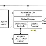
My last chip design at Intel was a GPU called the 82786and the architects of the chip wrote a virtual prototype using the MAINSAIL language. By using a virtual prototype they were able to:
- Simulate bus traffic, video display and video RAM
- Determine throughput
- Measure latency
- Verify that bus priorities were working
- Optimize the
…
Read More
My first job out of college was doing transistor-level circuit design, so I’m always curious about how companies are doing billion-transistor chip design and debug these days at the FPGA companies.
I spoke with Yaron Kretchmer,he works at Altera and manages the engineering infrastructure group where they have a compute… Read More
If your next SoC uses an ARM Cortex-A9 and has an industrial application, then you can save much design and debug time by using a prototyping platform. The price to prototype is quite affordable, and the methodology has a short learning curve. Bill Tomasan Aldec Research Engineer conducted a webinar today on: ARM Cortex SoC Prototyping… Read More
Standard cell library characterization has been around for decades, Synopsys has been offering Liberty NCXand Cadence has Virtuoso Foundation IP Characterization. What’s new is that Mentor Graphics acquired the Z Circuit technology for library characterization and has integrated it with the Eldo Classic circuit … Read More
With an HDL-based design methodology many IC engineers code in text languages like SystemVerilog and VHDL, so it’s only natural to use a text-based debug methodology. The expression that, “A picture is worth a thousand words” comes to my mind and in this case a visual debug approach is worth considering for … Read More
Image sensors are all around us with the cell phone being a popular example, and 35mm DSLR camera being another one. Last week I spoke with Kenton Veeder, an engineer at Senseeker that started his own image sensor IP and consulting services company. Instead of focusing on the consumer market, Kenton’s company does sensor … Read More
How do you learn new hardware design topics? I just got trained online about property-based verification for hardware designers using a free online class at Aldec. The material was created by Jerry Kaczynski, a Research Engineer at Aldec.
… Read More
At DAC 2012 we were hearing about the 20nm design ecosystem viability, however IC process technology never stands still so we have early process development going on now at the 10nm and 14nm nodes where FinFET technology is being touted. Earlier in February Vassilios Gerousis, a distinguished engineer at Cadence presented a session… Read More
The HSPICE circuit simulator has been around for decades and is widely used by IC designers worldwide, so I watched the HSPICE SIG by video today and summarize what happened. Engineers from Micron, Altera and AMD presented on how they are using HSPICE to model TSVs, IBiS-AMI models and SERDES, respectively.… Read More


TSMC CoWoS versus Intel EMIB Semiconductor Packaging