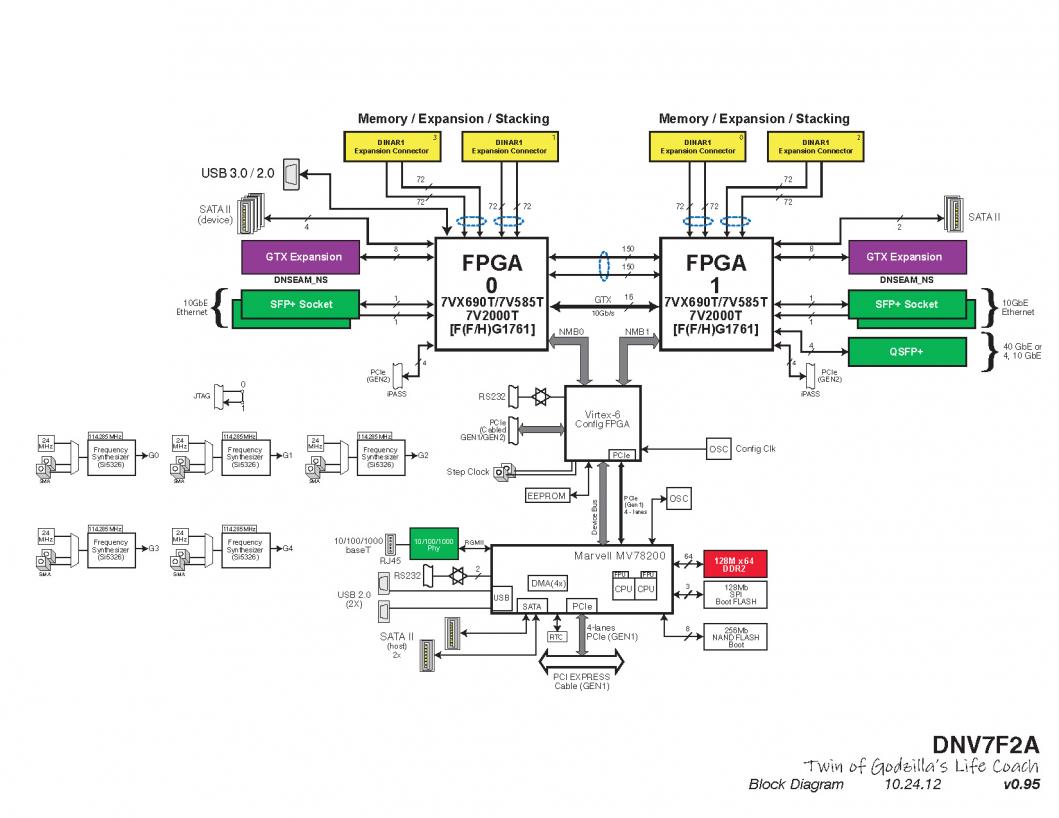
Collaboration in EDA is nothing new, however you may not be aware of how the Dini Group and Tektronix have worked together on an FPGA prototyping platform to address issues like debugging with full visibility across an entire multi-FPGA design. At SemiWiki we’ve blogged a couple of times so far about the new debug approach from Tektronix called Certus 2.0:
Debugging a 50M Gate design in an FPGA Prototype can take weeks of effort using old methods because of constraints caused by limited visibility across multiple FPGAs and multiple clock domains.

If you’re like me, then there’s nothing better than a workshop to see and touch a new technology to get up to speed. On Tuesday, December 11th there’s a workshop in Santa Clara that includes presentations by two experts:

Dr. Brad Quinton is the Chief Architect for the Embedded Instrumentation Group at Tektronix. He has over 15 years of engineering and research experience in the semiconductor industry. Quinton’s doctoral research at the University of British Columbia exploring on-chip debug architectures, was the inspiration behind the technology being developed by Veridae Systems Inc. which is now part of Tektronix Embedded Instrumentation Group.
Previously, Brad served as a consultant and senior design engineer at Teradici Corporation, and as a consultant at Altera, where he designed and debugged new devices. Prior to this he spent many years at PMC-Sierra, where, in his last role, he managed a multi-million dollar IC development from concept to market release.

Mike Dini founded the Dini Group back in 1990 and serves as President. The Dini Group offers FPGA Cluster Computing, High Performance Computing (HPC) and ASIC prototyping. Prior to Dini Group Mike did design and debug work at companies in medical electronics, computing and aircraft.
Outside of work you’ll probably see Mike creating vibrant artwork.
Mr. Dini earned both his MSEE and BSEE at UC Irvine.
Workshop Schedule
10:00 – 10:15 AM Registration
10:15 – 11:15 AM Understanding the options, strengths, and weaknesses of ASIC Prototyping hardware (The Dini Group)
- Emulation vs. FPGA
- Traditional FPGA debugging bottlenecks
11:15 – 12:00 PM Strategies for productive ASIC prototyping using multi-FPGA boards
12:00 – 12:30 PM Lunch
12:30 – 1:00 PM Example: How to implement “Full Visibility” for an ASIC Prototype of an SoC design
1:00 – 1:30 PM Strategies for how to debug a design on a ASIC Prototype with Full Visibility
1:30 – 1:45 PM Example: Design debug example of an SoC on an ASIC Prototype
1:45 – 2:00 PM Example: Performance optimization of an SoC on an ASIC Prototype
2:00 – 2:15 PM Deploying Full Visibility as a feature for software developers using ASIC Prototypes
2:15 – 2:30 PM Prize Drawing*
All attendees are eligible to win the $100 AMEX gift cards along with other prizes throughout the day. Lunch will be provided.
*Winners must be in attendance for the drawing at the conclusion of the seminar. You must register to attend and seating is limited to 40 attendees.


Solving the EDA tool fragmentation crisis