You are currently viewing SemiWiki as a guest which gives you limited access to the site. To view blog comments and experience other SemiWiki features you must be a registered member. Registration is fast, simple, and absolutely free so please,
join our community today!
Nvidia designs some of the most powerful graphics chips and systems in the world, so I’m always eager to learn more about their IC design methodology. This week I’ve had the chance to talk with Ting Ku, Director of Engineering at Nvidia about his DAC talkin the Apache booth in exactly two weeks from today. Registration… Read More
My 8 years as an IC circuit designer were at the transistor-level, so if that interests you as well then consider what there is to see from Cadence at DAC this year. IC design technology is changing quickly, so keeping up to date is important for your job security and continual education goals.
Here’s what I would recommend attending… Read More
As an engineer I learn new concepts best by seeing a demonstration, in this case it was a demo of how to optimize SoC performance by using an ASIC prototyping debug process. SoC designers that use FPGAs to prototype their new ASIC often encounter debug issues, like:
- Limited observability of internal nets required for debug, maybe
…
Read More
If you design with ARMCores and need to estimate dynamic power early in the flow, then consider what STMicroelectronics has done with their high performance, power-efficient subsystems. Anne Merlande is a Processor Micro Architecture technical expert, and will be presenting in Booth #1346 at DACon June 4th, 2:00PM. Her topic… Read More
My IC design career started at Intel with DRAM chips, so I’m very familiar with clockless design because we used self-timed techniques to get maximum performance. I remember blogging about an asynchronous design company called Tiempo back in 2010, while blogging at Chip Design Magazine. A few weeks ago there was a press … Read More
I love it when my Acura goes months and months without any major repair issue or computer-related glitches. Cars or networks only become reliable when they are designed and built for reliability. Freescale designs SoCs for advanced automotive and networking applications, and their engineers know much about the topics of power,… Read More
Cornelia Golovanovworks at LSI Corp in Pennsylvania and is an EMI expert that provides EDA tool and methodology advise to design groups. She earned a PhD in microelectronics and radioelectricity from the Institut national polytechnique de Grenoble, and joined Lucent out of school 12 years ago. We had a chance to talk by phone about… Read More
At DAC in just three weeks you can learn about which EDA vendors are supporting the latest UVM 1.1d (Universal Verification Methodology) standard as defined by Accellera. One of those EDA vendors is Aldec, and they have a 45 minute technical session that you can register for online. Space will fill up quickly, so get signed up sooner… Read More
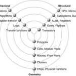
Thirty years ago in 1983 Professor Daniel Gajski and Kuhn created the now famous Y-Chart to show the various levels of abstraction in electronic system design:
We can still use this Y-Chart today because it still pertains to how engineers are doing their SoC designs. Along the Behavioral axis there is a need to know that each level… Read More
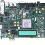
Most SoCs today are being prototyped in FPGA hardware before committing to costly IC fabrication. You could just design and build your own FPGA prototyping system, or instead choose something off the shelf and then concentrate on your core competence of SoC design.
Thanks to the FPGA vendors like Xilinx we now have FGPA prototyping… Read More


Intel, Musk, and the Tweet That Launched a 1000 Ships on a Becalmed Sea