You are currently viewing SemiWiki as a guest which gives you limited access to the site. To view blog comments and experience other SemiWiki features you must be a registered member. Registration is fast, simple, and absolutely free so please,
join our community today!
Freemium is the two words “free” and “premium” combined together, and many of us have enjoyed using freemium apps on our phones, tablets and desktop devices over the years. The concept is quite simple, you find an app that is useful, and download the free version, mostly to see if it operates as advertised,… Read More
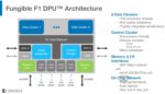
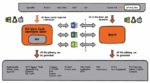
Domain specific processors are a mega-trend in the semiconductor industry, so we see new three letter acronyms like DPU, for Data Processing Unit. System level performance can actually be improved by moving some of the tasks away from the CPU. Companies like Xilinx (Alveo), Amazon (Nitro) and NVIDIA (BlueField) have been talking… Read More
According to the ESD Alliance, the single biggest revenue category in our industry is for semiconductor IP, so the concept of IP reuse is firmly established as a way to get complex products to market more quickly and reducing risk. On the flip side, with hundreds or even thousands of IP blocks in a complex SoC, how does a team, division… Read More
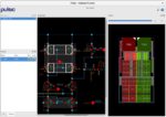
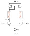
I viewed a recent webinar from Paul Clewes of Pulsic, and the topic was Balancing Analog Layout Parasitics in MOSFET Differential Pairs. This topic interests me, because back in 1982 I wrote my first IC layout automation tool at Intel that automatically created 15% of a GPU chip layout called the 82786, then joined Silicon Compilers… Read More
I can remember back in the 1980s how Apollo workstations were quite popular, because they accelerated the graphics display time for EDA tools much better than competitive hardware. Fast forward to 2022 and we have the same promise of speeding up EDA tools like PCB layout editing by using a GPU. At the 58th DAC there was a session called,… Read More
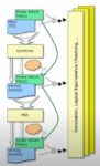
The Accellera organization created the concept of a Unified Power Format (UPF) back in 2006, and by 2007 they shared version 1.0 so that chip designers would have a standard way to communicate the power intentions of IP blocks and full chips. By 2009 the IEEE received the Accellera donation on UPF , reviewed multiple drafts and published… Read More
I’ve been following Neil Johnson on Twitter and LinkedIn for several years now, as he has written and shared so much about the IC design and verification process, both as a consultant and working at EDA vendors. His recent white paper for Siemens EDA caught my eye, so I took the time to read through the 10 page document to learn… Read More
I’ve followed the enthusiastic market acceptance of FPGA chips over the decades, and even semiconductor companies like Intel acquired Altera, while AMD tries to acquire Xilinx. The idea of field programmable logic makes a lot of sense for use in systems designs today, and it was inevitable that a company like Menta would… Read More
Walking the exhibit floors at DAC in December I spotted the familiar face of Anupam Bakshi, Founder and CEO of Agnisys, so I stopped by the booth to get an update on his EDA company. My first question for him was about the origin of the company name, Agnisys, and I found at that Agni means Fire in Sanskrit, one of the five elements.
The … Read More
With the Omicron variant of the COVID-19 virus in the news, there have been some big corporate names withdrawing from CES ( Peleton, Super73), however the cycling innovation companies assembled once again in Las Vegas this year for CES 2022. Data from statista show the strong growth in bicycle revenues in March 2020, when the pandemic… Read More


Captain America: Can Elon Musk Save America’s Chip Manufacturing Industry?