You are currently viewing SemiWiki as a guest which gives you limited access to the site. To view blog comments and experience other SemiWiki features you must be a registered member. Registration is fast, simple, and absolutely free so please,
join our community today!
CES 2012 Trip Wrap-Up!by Daniel Nenni on 01-15-2012 at 4:00 pmCategories: Events
The Consumer Electronics Show (CES) in Las Vegas is the premier electronics gadget exposition, a window into what we will be spending our hard earned money on next Christmas. Personally, I go to CES every year to try and guess what new innovative technology will drive future semiconductor design and manufacturing. Last year I bet… Read More
A common discussion amongst semiconductor professionals is the ROI of development activity in India. An interesting number I remember hearing at Virage Logic was that the development groups in India had a 30%+ turnover rate. Is that still the case? If so, that is very hard on the ROI.
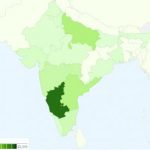
Here are the 2012 SemiWiki geographical statistics… Read More
Altera recently introduced versions of their new Arria® and Cyclone® V FPGA families that incorporates a dual ARM®Cortex™-A9 MPCore hard core. These parts are particularly interesting to NARD as it’s consistent with the NARD concept of offering platforms unified by a common ARM® host core and a variety of controller/coprocessor… Read More
Just how many hands have touched your SoC design by the time it goes to manufacturing? Clearly the more hands that touch it, the more complex the design is, making it more difficult to meet your product requirements. The commercial semiconductor IP dilemma is that not only are you using the same IP as your competitors, you are exponentially… Read More
It has been an amazing year for us so we wanted to thank you all for being a part of the Semiconductor Wiki Project!
The SemiWiki Bloggers are off this week and will return the first week of January. During this time there will be a major SemiWiki software update. There will be performance upgrades and lots of new features to enhance the… Read More
During my annual holiday meal with one of my favorite EDA icons some rather bold predictions were made. On his side it was more of what he would LIKE to see happen, on my side it was more of what will HAVE to happen for the semiconductor ecosystem to thrive in the coming years.
Mike Gianfagna (Viva Italia!) spent 15+ years with RCA/GE Semiconductor… Read More
Conspiracy theories abound! The inside story of the Synopsys (SNPS) acquisition of Magma (LAVA) brings us back to the 1990’s tech boom with shady investment bankers and pump/dump schemes. After scanning my memory banks and digging around Silicon Valley for skeletons with a backhoe here is what I found out:
The Commission… Read More
Just returning from my monthly trip to Taiwan and I find myself energized! Semiconductors, EDA, and the ASIC business have never been more exciting! The travel itself is not so exciting but since I make frequent trips the airline and hotel treat me like a king. And let me tell you, it is good to be a king!
Speaking of royalty, I saw Dr. … Read More
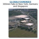
Some call it co-opetition (collaborative competition), some call it keeping your enemies close. Others call it for what it is, unfair competition and/or other types of legally actionable behavior. GlobalFoundries calls it“Fab Syncing”, which in reality will SINK their FABS!
“With this new collaboration, we are making one … Read More
Interesting story, for my wife’s 50th birthday we went to Las Vegas to see Sir Elton John in concert. My wife is an Elton fan and this may be her last chance to see him live so off we went. I saw Elton and Billy Joel in a dueling piano concert a while back and it was simply amazing! The underlying purpose of the trip however was to earn “Perfect… Read More


Captain America: Can Elon Musk Save America’s Chip Manufacturing Industry?