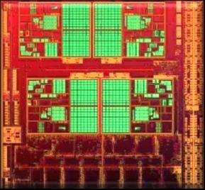
GLOBALFOUNDRIES showed off its 28nm design ecosystem at #48DAC last week in San Diego. The company featured a full design ecosystem for its 28nm High-k Metal Gate (HKMG) technology, including silicon-validated flows, process design kits (PDKs), design-for-manufacturing (DFM), and intellectual property (IP) in partnership with industry leaders. 28nm is the second node of HKMG production for GFI with 32nm AMD Llano dice already in the field. CPU’s and GPU’s are the most difficult designs to manufacture and Llano is both.

In case you missed it, here is a reprint of a 28nm HKMG overview from GFI just prior to #48DAC:
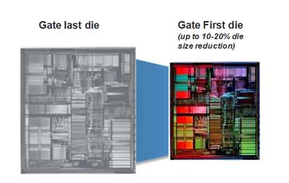
High-K/Metal Gate (HKMG) is one of the most significant innovations in CMOS fabrication since the development of silicon VLSI. The 28nm technology is designed for the next generation of mobile smart devices demanding faster GHz processing speeds, lower standby power and longer battery life. To meet these demands, the 32/28nm HKMG solution is a “Gate-First” approach that shares the process flow, design flexibility, design elements and benefits of all previous nodes based upon poly SiON gates. This solution is far superior to present alternatives in scalability (performance, power, die size, design compatibility), cost (a typical foundry customer will save tens of millions of dollars over the course of a 28nm vs. 40nm product portfolio lifecycle) and manufacturability

GLOBALFOUNDRIES’ 28nm-SLP technology is the low-power CMOS offering delivered on a bulk-silicon substrate for mobile applications. Relative to other 28nm technologies, it achieves its lower cost platform by substantially reducing process complexity and mask counts. It offers design flexibility with multi-channel length capability and the ultimate in small die size. Available options include multiple SRAM bit cells for high density and high performance.
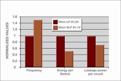
Since this process downsizes the footprint and power utilization, it optimizes energy efficiency, which translates into significantly longer battery run times and fewer recharge cycles; the benchmark of wireless devices moving forward. The gate-first HKMG process utilizes a functional voltage below 0.8V, scaling 28nm performance and power proportionately against 40nm-LP poly SiON. Overall performance gains include a 49% higher frequency capability, a 44% reduction in energy utilization per switch and >25% reduction in leakage power per circuit (see Figure 1). The 28nm- SLP, Gate-First process also supports standard overdrive practices providing additional performance and flexibility gains for a broader application base (wireless AND wired).
A significant benefit of 28nm-SLP technology is that it provides hefty analog “headroom” (Vcc-Vt) and low noise performance relative to the offerings of other foundries. Gate-First enables a reduction in design complexity by preserving design architecture and layout style, thereby leveraging design investments with IP reuse. This design compatibility helps reduce the overall risks of adopting 28nm.
The Super-Low Vt option provides a performance boost over traditional Vts at a given process node, opening the door for greater than 2GHz performance. The resulting performance boost with a minimal increase in power makes this option attractive to applications with specific thermal requirements that still require the largest performance envelope.

Conclusions
The 28nm low-power technology presents tremendous value over the 40nm process, for the industry. It achieves substantially smaller die size than competing foundry offerings. Reduced risk is a hallmark of this low-power technology. It facilitates proven high-volume manufacturing at multiple Common Platform Alliance locations globally as well as a fully enabled design ecosystem with IP and tools and proven design flows, while sustaining the industry design style, flexibility and infrastructure utilized at 40nm and all previous technology nodes. This available technology provides superior performance and analog headroom for wider design margin and lower manufacturing cost.

The GFI Concurrent Newsletter is HERE.
Note: To read/write comments you must be logged in
Share this post via:


The Intel Common Platform Foundry Alliance