





Every generation of semiconductor innovation has relied on one fundamental principle: before a technology can be manufactured at scale, it must first be understood. That understanding comes through characterization.
For decades, characterization enabled process learning. It helped engineers understand transistor behavior, quantify process variation, qualify new technologies, and improve yield. Every major advance from strained silicon and high-k metal gate to FinFETs and Gate-All-Around transistors, all required increasingly sophisticated characterization techniques.
Today, the challenge is different. As semiconductor innovation shifts from optimizing transistors to optimizing heterogeneous systems, characterization must evolve as well. Its role is no longer limited to enabling process learning; it is becoming the foundation for production control.
Ramune Nagisetty, Enterprise Account Director at PDF Solutions, explored this evolution during a presentation at the IMAPS CHIPcon 2026 conference.
Innovation Has Moved Beyond Silicon
Moore’s Law, the economic observation that cost per transistor would reduce by about 50% every two years, has evolved over time. Initially, it was closely associated with the dimensional scaling of planar transistors and associated voltage and power reduction, which was called Dennard scaling. However, traditional Dennard scaling slowed and ended in the early 2000s. Material innovations, such as strained silicon, hiK metal gate, as well as new transistor architectures such as FinFET and Gate-All-Around transistors have continued to deliver performance, power, and area (PPA) improvements at reasonable cost.
In parallel, design technology co-optimization (DTCO) has evolved as a method to improve PPA by optimizing standard cells and IP block layouts. More recently, System Technology Co-Optimization (STCO) has extended optimization beyond the die by combining multiple specialized chiplets into an advanced package.
Packaging Has Become Foundational to Architecture and Design
Packaging is no longer simply the final manufacturing step. It influences power delivery, thermal performance, bandwidth, reliability, and overall system architecture. As advanced packaging adopts increasingly sophisticated manufacturing techniques, the distinction between front-end silicon and back-end packaging continues to blur. The result is a shift from optimizing individual dies to optimizing complete systems.
Innovation Creates New Manufacturing Challenges
Heterogeneous integration unlocks significant system-level benefits, but it also introduces new interactions between devices, packages, materials, and manufacturing processes. Understanding those interactions requires characterization to extend beyond its traditional role.
Chiplets Redefine Manufacturing Complexity
Chiplets improve design flexibility, accelerate product development, and allow each function to use the most appropriate process technology. They also fundamentally change manufacturing.
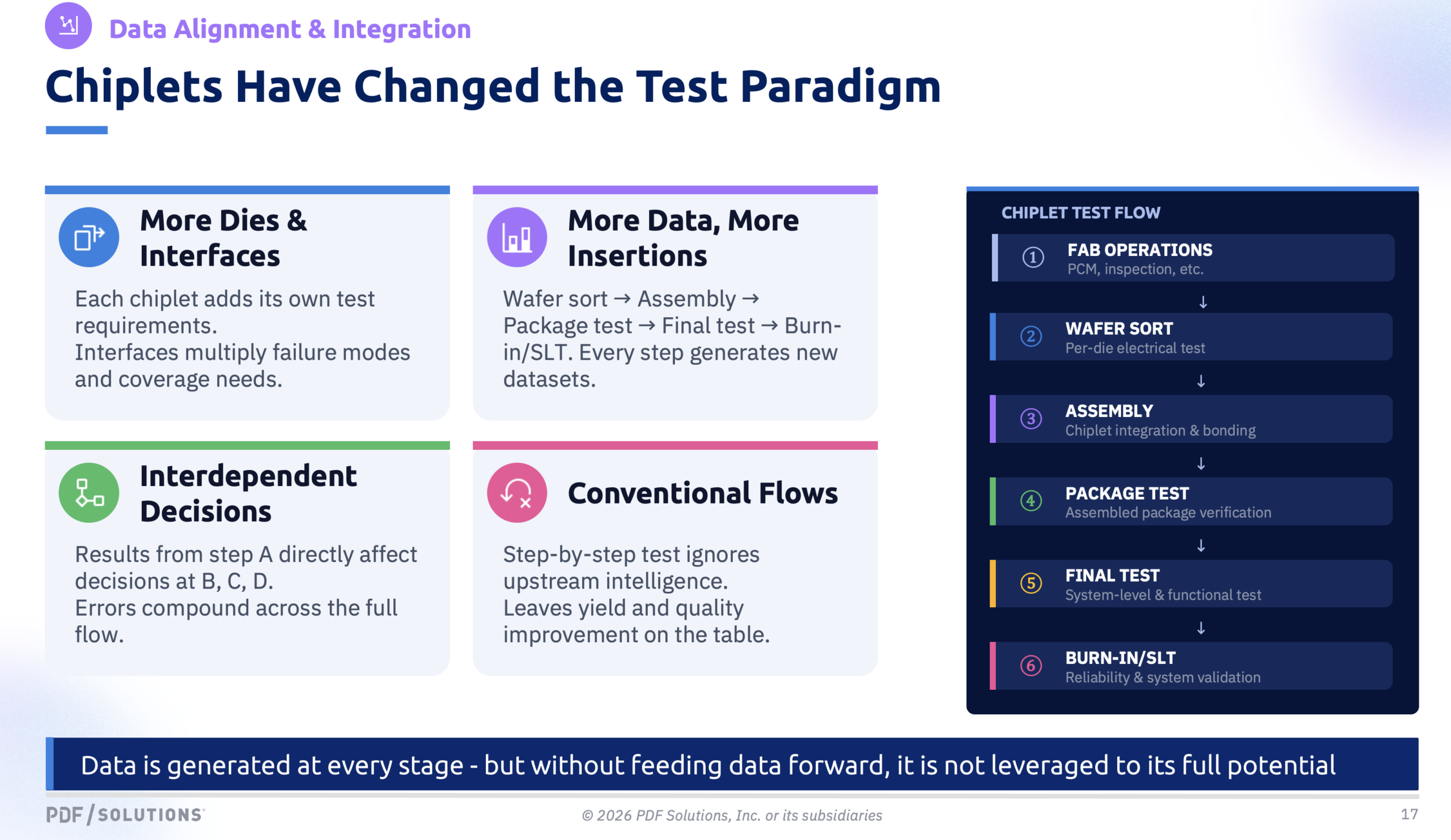
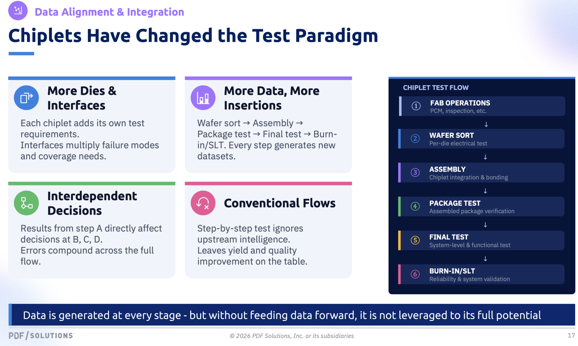
Manufacturing Is No Longer Linear
Instead of a single manufacturing flow, heterogeneous systems combine dies from multiple foundries, process nodes, and suppliers before converging during advanced packaging. From there, products progress through assembly, package test, burn-in, final test, and system validation. Each stage generates valuable manufacturing knowledge.
Complexity Grows Faster Than Die Count
Every additional chiplet increases interfaces, failure mechanisms, test insertions, and manufacturing decisions. At the same time, manufacturing knowledge becomes fragmented across foundries, OSATs, and test operations. The challenge is not just integrating silicon. It is integrating manufacturing knowledge.
Characterization Must Become System-Aware
Traditional characterization focused on understanding process technology. Heterogeneous systems require it to understand system behavior.
New Failure Mechanisms Require New Measurements
Advanced packaging introduces interactions that conventional silicon characterization cannot fully capture. Mechanical stress, thermal coupling, through-silicon vias, hybrid bonding, package materials, and cross-layer effects all influence system performance and reliability.
Characterization Must Follow the Manufacturing Flow
Short-flow characterization remains essential, but it must be complemented by full-flow test vehicles that capture interactions introduced during wafer thinning, die singulation, package assembly, and final integration.
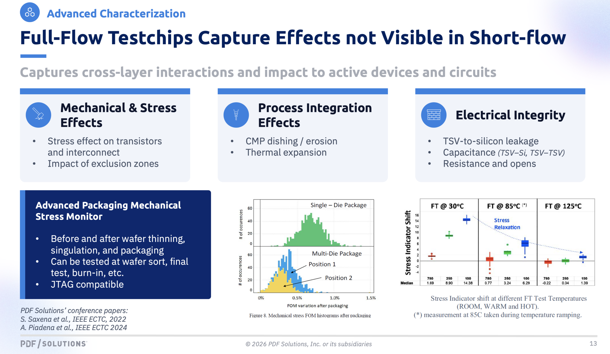
Characterization is no longer confined to qualifying a manufacturing process. It must characterize the behavior of complete heterogeneous systems throughout the manufacturing lifecycle.
Manufacturing’s Missing Link: Data and Knowledge Continuity
As characterization expands, so does the amount of manufacturing knowledge it generates.
Every Manufacturing Stage Learns Something
Wafer fabrication, wafer sort, assembly, package test, burn-in, and system-level validation each reveal different aspects of device behavior. Together, they create a comprehensive picture of every device’s manufacturing history.
But the Knowledge Rarely Travels
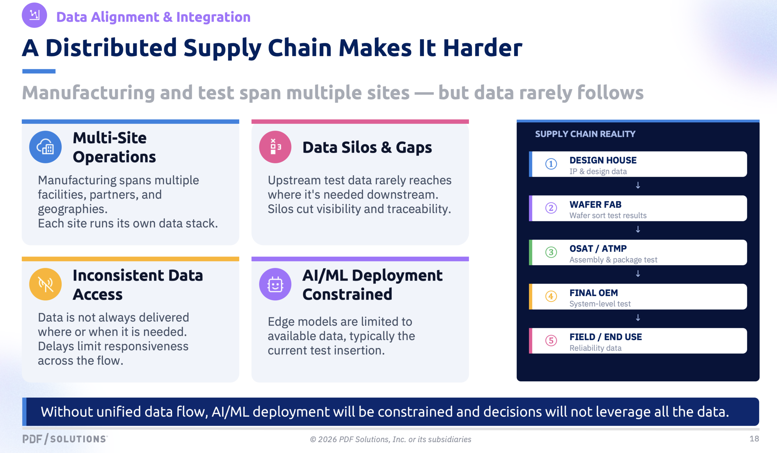
Too often, that knowledge remains trapped within individual manufacturing stages or organizations. As products move through foundries, OSATs, and test facilities, valuable context is lost, forcing downstream teams to rediscover what upstream processes already learned.
The industry has a data and knowledge continuity challenge.
From Characterization to Production Intelligence
Closing that knowledge gap requires more than collecting additional data. It requires transforming characterization into production intelligence.
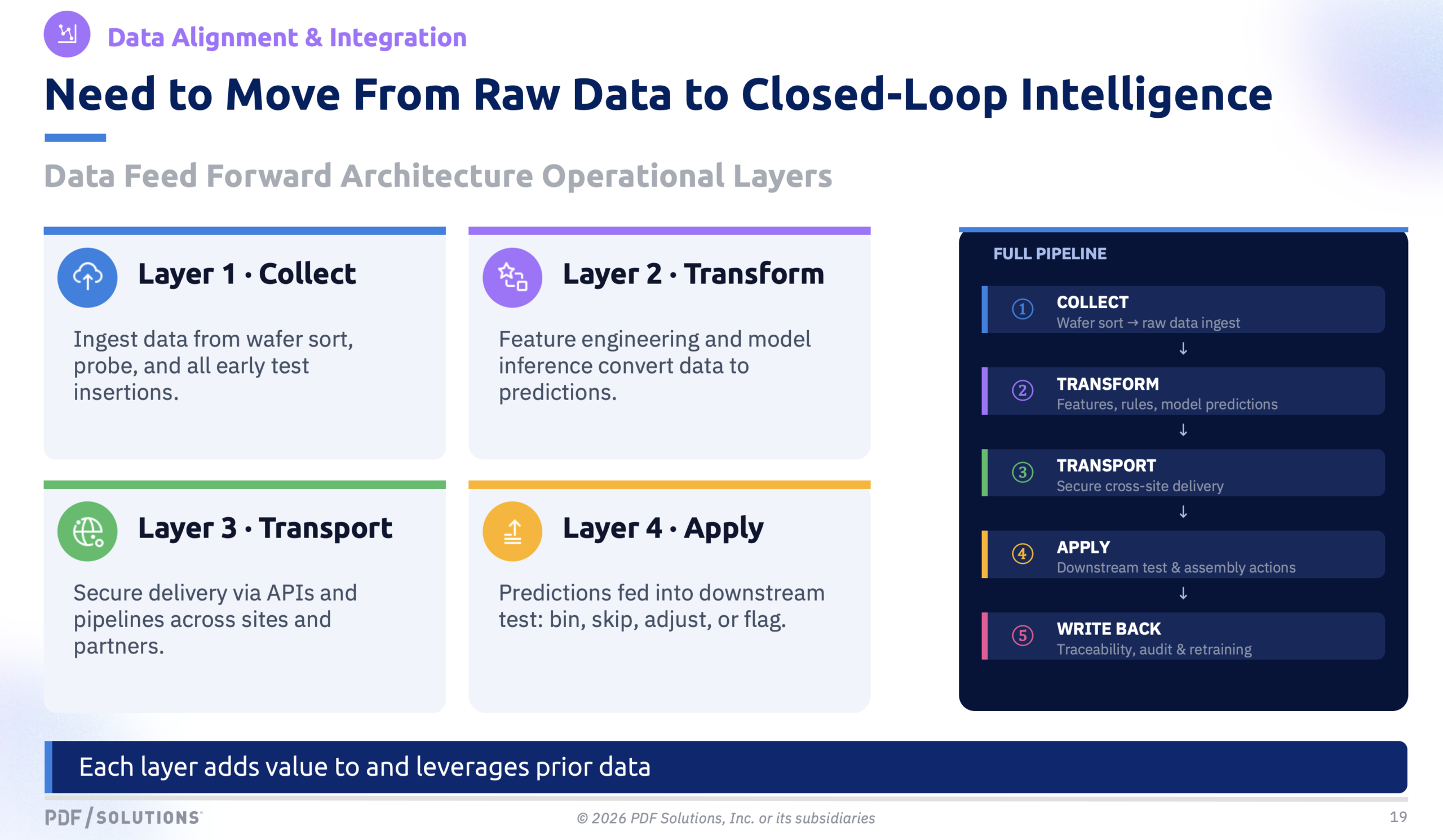
Connecting Knowledge Across the Manufacturing Flow
Connected data, unit-level traceability, and feed-forward analytics enable insights generated during characterization and early test insertions to guide downstream manufacturing decisions. Rather than treating each manufacturing stage as an isolated checkpoint, production becomes a continuous learning system. (Readers interested in the underlying Data Feed Forward (DFF) architecture and its role in AI-driven semiconductor manufacturing can find more details in an earlier SemiWiki post and in this keynote presentation.)
Learning Becomes a Manufacturing Capability
The result is adaptive testing, improved yield prediction, earlier defect detection, more accurate performance binning, and AI models that learn from a device’s complete manufacturing history rather than isolated snapshots.
Characterization no longer ends with measurement. It becomes the intelligence layer that enables production control.
Summary
For decades, competitive advantage came from understanding increasingly sophisticated manufacturing processes. Tomorrow, it will come from understanding increasingly sophisticated manufacturing systems.
The leaders in heterogeneous integration will not simply build better chiplets or more advanced packages. They will be the companies that best preserve, connect, and operationalize manufacturing knowledge across the entire production flow.
Also Read:
The Yield Partnership: Intel and PDF Solutions Tackle Advanced Nodes
Feed Forward Intelligence: Enabling Testability in the Chiplets Era
From Point Solutions to Agentic AI Ecosystems: Semiconductor Process Control Depends on Its Past
Share this post via:



Comments
There are no comments yet.
You must register or log in to view/post comments.