New MIPI protocols: Unipro, LLI and CSI3 over MPHY.
Gabriele ZARRI, Moshik RUBIN, Cadence
Sophia Antipolis, France SAME 2012 Conference – October 2 & 3, 2012 2
Abstract:
With more than 50% of the world‟s population using cellular phones and the growing number of devices that go mobile, from game consoles and media player to tablets and smartphones, the demand for higher bandwidth, less power consumption and, of course, reduced cost – led a consortium of companies to form the MIPI Alliance. The goal of the MIPI Alliance is to define a suite of interfaces for use in mobile and consumer products, covering all the different aspects including Battery signalling (MIPI BIF), Radio (MIPI DigRF and RFFE), Digital audio (MIPI SLIMBus), Off-die memory sharing capabilities (MIPI LLI), Camera sensors (MIPI CSI) and Displays (MIPI DSI).
Most of those protocols use common layers (like Unipro and/or M-PHY) that guarantee a consistent interface that enables RTL reuse and optimization. Pre-silicon Verification of MIPI complaint devices is challenging and demanding; the layered structure of the specifications and the rapid pace of new revisions and features require a flexible, modular and advanced testbench which is well beyond the ability of the traditional directed testing verification scheme that most designers employ.
This paper will present an advanced verification methodology and offer some practical guidelines for pre-silicon verification of MIPI devices. Real-world verification environments used in actual verification of MIPI devices will be reviewed. The mobile market requirements are expanding quickly in terms of performances for battery duration, bandwidth needs, video capabilities like 3D, etc…
The goal of the MIPI Alliance is to define a suite of interfaces for use in mobile and consumer products, covering all the different aspects including Battery signalling (MIPI BIF), Radio (MIPI DigRF and RFFE), Digital audio (MIPI SLIMBus), Off-die memory sharing capabilities
(MIPI LLI), Camera sensors (MIPI CSI) and Displays (MIPI DSI).
Most of those protocols use common layers (like Unipro and/or M-PHY) that guarantee a consistent interface which enables RTL reuse and optimization Old standards needed to evolve in order to enable the new market requirements. CSI-2 protocol, targeting camera interfaces, was one of the first MIPI to be well adopted by the IC developers but was based on a PHY that could support up to 1Gpbs per lane ; now with increased bandwidth requirements, a new version of the protocol (CSI3) was created in order to leverage Unipro layered approach over a new phy (MPHY) that can support up to 6Gbps per lane with a reduced number of wires.
Since we are now moving towards multiple videos flows merging into the same screen, exploding the current video performance capabilities, the display protocol (DSI-2) is currently following the same trend and will soon be able to connect to Unipro/MPHY layers as well.
The attractive performance and the robust implementation of the MIPI protocols have now gone beyond the MIPI family boundaries and we can see other standards bodies taking advantage of MIPI protocols, layering application driven protocols on top of MIPI Unipro and/or M-PHY. The recent examples are JEDEC‟s UFS flash memory, implemented on top of MIPI M-PHY, and SSIC (Superspeed Inter-Chip), enabling USB 3.0 on top of MIPI M-PHY.
This fact introduces the needs of advanced flexibility in the protocols, which now have to be interfaced with other industry standards, making the number of possible interfaces configurations even wider. Now with such tight requirements something else becomes urgent: improving cost and resources sharing across dies.
For example, phone memories are not fully used within the same chip and until now every dye had to have its own leading to a much un-optimized implementation and higher cost.
One of the newest protocols of the MIPI family, is a low latency interface (LLI) which allows an off-die memory sharing between a processor chip and a companion one, guaranteeing that the same memory could be accessed from off-dye and therefore sparing the cost of additional memories by fully reusing the same among chips.
As its “big brother” Unipro, LLI is using as well the M-PHY protocol as a physical layer.
This makes M-PHY protocol a well established new standard for general purpose chip-to-chip interface.
The introduction of many, new and advanced specifications, with high dependencies between them, brings along new verification and testing challenges that traditional pre-silicon verification techniques cannot address.
In order to keep up with the latest standards, mobile SoC and systems manufacturers need solutions that can test the functionality of their designs―quickly, accurately, and cost-efficiently. Pre-silicon Verification of MIPI complaint devices is challenging and demanding; the layered structure of the specifications and the rapid pace of new revisions and features require a flexible, modular and advanced testbench which is well beyond the ability of the traditional directed testing verification scheme that most designers employ.
In a layered-protocol verification IP, the major challenge is the ability to provide enough flexibility from the upper layers without reducing the effectiveness of the random approach. In a typical example, if IP developers are interested in a standalone verification of every and each layer of their IP, their activity might be heavily impacted as the protocols pile up : an MPHY verification engineer requires the ability of generating all kind of traffic on the physical lanes, which will guarantee a full coverage of the protocol, including error injection mechanism to guarantee enough robustness. But based on the upper layer used on top (LLI, Unipro, DigRF), the kind of K-symbols required, the width of the symbol, the physical transmission mode might change. The challenge for a VIP developer in this case would be to provide a multi-purpose verification IP capable of containing all kind of configurable implementation fitting all user models.
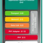
When using this same PHY under Unipro, the verification activity will actually depend on the confidence of the MPHY IP itself. Unipro protocol contains many layers, that go from the Physical Adapter(PA), to the Data Link Layer (DLL), to the Network Layer (NL), up to the Transport Layer (TL). On top of it, we can position the Application Layer, which can consist, for example, in the camera layer (CSI-3).
The suggested verification approach would be bottom –up, i.e. starting from the Physical Adapter layer ;
The major features that could be verified would be, for example, the link startup, the link configuration (and re-initialization), and correct sending/reception of PACP frames. Once this layer is correctly verified we can move to the next one, which will focus mostly for all classes of traffic on Flow control, arbitration schemes, data AFC and NAC transmissions.
While the verification of the NL would focus on the DeviceID information, and to send/receive the packets (with short and long header), the TL verification would address the connection management for multiple ports (C-Ports), the address translation, the flow control when present (end-to-end flow control (E2EFC) or CSD), and the segmentation/reassembly.
If every layer has its own specificities and could be verified only focusing on its own features/capabilities, it would be interesting to be able to control from an upper layer, like the TL, all kind of items belonging to the NL and the DLL layers.
If from a verification IP a random generation of a TL segment will take care of pseudo-randomizing all the rest of the layers traffic down to the MPHY symbols (according to the upper layer constraints and the protocols‟ specification), there is often the need of fully controlling the scenario which is going to be generated by the Verification IP : a simple reason might be the DUT readiness, as during the development phase some functionalities might not be implemented yet, and a more „direct test‟ approach might be required.
But if this is an easy task with a limited number of parameters in a single-layered protocol, in our example it is not easy to know in advance if a control of the MPHY capabilities is required from a Unipro TL, or if a control only on the direct layers beneath him (NL and DLL) will be enough.
This verification choices are often dictated by the confidence of the modules verification : if an MPHY IP is verified in-house by a team sit right next door, the verification engineer will be more confident than if the IP has been purchased by a third party over which he didn‟t have visibility during the IP level verification.
The same rationale applies to other protocols, like LLI. When the LLI receives an error from the MPHY, it‟s supposed start a retransmission mechanism. During the LLI IP verification (pictured below as LLI Device Under Test) the traffic is generated by LLI TL layer.
Now, there are many MPHY errors that can be the source of the error signal toggling from the MPHY up to LLI layer parallel interface. The only way of testing the retransmission from the LLI protocol stack is to inject traffic from the TL-layer while controlling the MPHY error generation.
It is clear that in a layered verification activity, the only way to guarantee a full coverage is to provide to the users a way of controlling all layers, which makes a VIP user interface extremely complete and therefore complex to create in a easy-to-use manner.
The purpose of the article was to give an overview of emerging MIPI standards, with focus on advanced pre-silicon verification methodologies and techniques to test MIPI protocol compliance, providing practical guidelines for pre-silicon verification of MIPI devices.
Moshik Rubinis Senior Product Line Manager for Verification IP (VIP) at Cadence. He has been in the EDA industry for over ten years. He served as Verification IP Engineering manager at Verisity and now manages several protocols within Cadence’s VIP portfolio including PCIe, HDMI and MIPI verification IPs. Mr. Rubin holds a BS in Computer Engineering from the Technion – Israel Institute of Technology as well as an MBA from Tel-Aviv University’s Recanati Graduate School of Business.
Gabriele ZARRI
Gabriele Zarriis a Verification IP Solutions and Deployment Architect, in charge of OCP and MIPI product deployment worldwide and responsible for Cadence’s VIP portfolio deployment for Europe. He has been in the EDA industry for ten years serving different positions in Project and Product Management for Verification IPs.
He is currently chairing the Functional Verification Working Group for the OCP International Partnership (OCP-IP).
Mr. Zarri holds a MS in Electronics and Telecommunications from the Sophia-Antipolis University.