Bronco Webinar 800x100 1

Internet of Things, My Bluetooth Headset

Internet of Things, My Bluetooth Headset
by Daniel Payne on 11-20-2012 at 8:42 pm

A catchy phrase used by bloggers and journalists these days is “Internet of Things“, or IoT if you prefer acronyms. All of this is made possible by EDA tools in the hands of SoC designers to create useful products like my Jawbone ICON bluetooth headset. Tonight I discovered that I could customize my bluetooth headset by installing some software on my MacBook Pro and also on my Android-powered Samsung Infuse smart phone. Continue reading “Internet of Things, My Bluetooth Headset”


Apache on Signal Integrity

Apache on Signal Integrity
by Paul McLellan on 11-20-2012 at 1:09 pm

Matt Elmore has a two-part blog about the growing complexity of signal integrity analysis, both on the chip itself and the increasingly complex analysis required to make sure that signals (and power) get in and out of the chip from the board cleanly, especially to memory, which requires simultaneous analysis of chip-package-system or CPS. Part1 Part2

A particular problem is analyzing simultaneously switching outputs (SSO) when using DDR to access off-chip memory. The big challenge in CPS signal integrity simulation is the sheer complexity. It is simply not possible just to take all the relevant parts of the design and throw them into a SPICE simulator. The power grid alone may have millions of nodes. One potential solution is to divide the simulation up into smaller pieces, such as analyzing each byte separately, but that means that interaction between adjacent bytes is assumed to be irrelevant, which might turn out to be a very expensive assumption if wrong. The reality is SSO issues are a global problem (many outputs switching together affect the power supply voltage across all I/Os and indeed the core of the chip).

A better approach is to accurately capture all the relevant characteristics in a considerably reduced model, with enormously shorter runtime. This has been possible for the power delivery network (PDN) for some time but now channel model reduction advances are able to retain the accuracy required while modeling the whole system from end to end: die, package, PCB, memory. Previous generation simulation technology is just inadequate to simulate full I/O b banks (128+ bits) in a reasonable time. So accurate modeling is the key to successful high speed (17Gb/s) interface designs.

I/O buffer performance is highly susceptible to on-die power noise. I/O buffers firing simultaneously will draw current from the battery in sharp increments, resulting in voltage drop and a shared fluctuation of effective supply levels (Vdd-Vss). In order to take this into account, the power/ground routing of the I/O ring must also be modeled. Leveraging a chip power model with power/ground extraction and reduction technology helps create a compact model of the resistive, capacitive, and inductive coupling of the I/O ring power grid.

SPICE is still the de facto simulation engine for DDR signal and power integrity simulation. Using a tool, such as Apache’s Sentinel-SSO solution for example, helps bundle these modeling technologies together in a single interface designed for signal integrity. The netlisting and connection of these models is automated by the tool and fed into the SPICE simulator of choice. After simulation, the timing, jitter, and noise waveforms and metrics are displayed for review. Previously, full-channel SSO simulations of the chip, package, and PCB were unobtainable. However, designers now have advanced modeling technology to sign-off their systems with reasonable turnaround times.


EDS Fair: Dateline Yohohama

EDS Fair: Dateline Yohohama
by Paul McLellan on 11-20-2012 at 12:22 pm

Electronic Design and Solutions Fair (EDSF) was held in Yokohama Japan from Wednesday to Friday last week. It was held at the Pacifico Hotel, somewhere I have stayed several times, not far from the Yokohama branch of Hard Rock Cafe and, what used to be at least, the biggest ferris-wheel in the world.

Atrenta was one of the many companies at EDSF2012. The EDS fair consists, for the second year, of a combination of what used to be a pure EDA show and the larger embedded show. Since Japan tends to be in the forefront of systems thinking, with Europe coming next and the US bringing up the rear, this combination is good since it brings in people from across the whole spectrum of design, not just a succession of CAD managers from the usual suspects. This is especially important for Atrenta since they are focused on doing design at a higher level with IP and software IP combined together to form systems.

Atrenta managed to generate a good supply of high-quality leads, each qualified by either an AE or a salesperson (so this doesn’t include students, press etc). Just like SemiWiki, students, press, PR and everyone are all very welcome but in the end it is the real design and embedded engineers who are the most important audience.

One thing that worked very well was the use of iPads as a way for customers to receive a deeper understanding of Atrenta’s products. They ported product presentation pdfs onto 8 iPads. In addition to salespeople and AEs using them as a tool to explain Atrenta’s products, the iPads also provided a venue for customers to get a deeper understanding of their products than they would typically receive from perusing a panel. It proved to be very effective as it allowed them to engaged with more customers than by using demos alone.

In terms of product interest, the highest was with BugScope. We believe this to be a combination of existing customers wanting to know about our newest product as well as designers looking for solutions to their verification challenges. Following closely behind where: SpyGlass CDC, SpyGlass for FPGA (we had a presentation highlighting SpyGlass plus CDC combined with the Xilinx Vivado support), and SpyGlass Power.

Meanwhile, back on this side of the Pacific, Ed Sperling had one of his round tables on the challenges of 3D, new process nodes. Venki Venkatesh of Atrenta was one of the participants. I’ve participated myself in a couple of Ed’s round tables. Basically he records the whole thing and then transcribes it (himself, it is so technical you can’t just give it to a secretary-type), cleans up the ums and ers and publishes it pretty much verbatim. You can find this one here. One of themes, as I’ve been pointing out, is that people are going to stay on 28nm as long as possible, that there is no rush to 20nm since the costs are a challenge (never mind the technical challenges).

There is also a short video version with the same people around the table here.


How much SRAM proportion could be integrated in SoC at 20 nm and below?

How much SRAM proportion could be integrated in SoC at 20 nm and below?
by Eric Esteve on 11-20-2012 at 4:45 am

Once upon a time, ASIC designers were integrating memories in their design (using a memory compiler being part of the design tools provided by the ASIC vendor), then they had to make the memory observable, controllable… and start developing the test program for the function, not a very enthusiastic task (“AAAA” and “5555” and other vectors), look for the test coverage, and try to be creative to reach the expected 99,99% magic number. I agree that this was long time ago, but when looking back to this old time, you realize how powerful is DesignWare Self-Test and Repair (STAR) Memory System from Synopsys, initially developed by Virage Logic. Today we are talking about the version 5 of the tool. Moreover, since the year 2000’s, most of the ASIC vendors are externally sourcing the SRAM compiler (to Virage Logic at that time…), ASIC designer is taking benefit of faster, denser memories with Built-In-Self-Test (BIST) integrated.

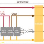
According with Semico, the number of processors integrated into a single SoC is growing (left caption, even if I am not sure that 16 processor per SoC is the standard in 2012 for every SoC, this is certainly the case with Application Processor for smartphone or Set-Top-Box), and, as a matter of fact, processor cache size is growing (middle caption), leading memory to dominate chip area, as we can see on the right of the picture. Leading to an immediate consequence on the SoC yield: it would dramatically decrease, if… the designer don’t use repair capability, like for example this offered by the STAR product (for Self-Test and Repair). Another precision about STAR version 5: unlike the previous version sold by Virage Logic, the tool can be available for a memory generated by a compiler coming from any vendor. Last, but not least precision, STAR Memory System 5 is targeted for designs implemented at 20-nm and below technologies.

You may want to challenge the assertion claiming that SoC yield would be severely impacted when integrating higher SRAM proportion within IC at 20nm and below? Thus, just have a look at the above pictures:

  • Double patterning introduces variation from overlay shift,
  • Voltage Scaling induces local variation with voltage, and
  • Random Dopant Fluctuation generates global and local Vth variation

These process variations become significant at 20nm, causing bit failure. Implementing SRAM in a system (on Chip) is no more a “drag and drop” action, the designer has to also take into account a solid (automated) test generation, as well as to introduce repair capability, as the risk of failure is statistically… a certitude.

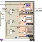
STAR Memory System 5 can be implemented for SRAM, as already mentioned, and also for ROM, Register File or Content Addressable Memory (CAM). The designer will implement a specific wrapper interfacing with the various memories, and a real memory sub-system is created, comprising a master and several slaves. The master, SMS Server, is connected to the outside world by a Test Access Port (TAP), and to several slaves (SMS Processors) through an IEEE 1500 normalized Bus. Each of the SMS Processors is connected to various memories (can be Single or Dual Port SRAM or Register Files) through the wrappers. Indeed, the test bench generation and the above described insertion are completely automated by STAR Memory System 5, also allowing performing diagnosis and redundancy analysis.

After running the test program on processed wafers, the failure diagnosis and fault classification will allow implementing redundancy, thanks to the Efuse box (Top right of the SoC block diagram), and dramatically increase the final SoC yield, as we can see per the image below.

To summarize, we have listed some unique features of the DesignWare STAR Memory System 5:

  • Performance and area optimized architecture to efficiently test & repair thousands of memories with smaller area and less routing congestion

  • Automated IP creation, hierarchical SoC insertion, integration, verification and tester-ready pattern generation
  • Hardened STAR Memory System IP with Synopsys’ DesignWare memories enabling faster design closure, higher performance, higher ATPG coverage, smaller area and reduced power.
  • Advanced failure analysis with logical/physical failed bitmaps, XY coordinates of failing bit cells and fault classification

Important to notice, this new version offers:

  • New optimized memory test and repair algorithms to efficiently address memory defects, including process variation faults and resistive faults, at 20-nm and below
  • New hierarchical architecture reducing test & repair area by 30% compared with the previous generation
  • Hierarchical implementation and validation accelerating design cycles by allowing incremental generation, integration and verification of test and repair IP at various design hierarchy
  • Support for test interfaces of high-performance processor cores maximizes design productivity and SoC performance, see below:

You may want to read the official Press Release from Synopsys about STAR Memory System 5

Eric Esteve


Andy Bryant Will Now Lead Intel Into The Foundry Era

Andy Bryant Will Now Lead Intel Into The Foundry Era
by Ed McKernan on 11-19-2012 at 12:30 pm

The announcement that Paul Otellini will step down in May 2013 is extraordinary in the history of the way Intel makes CEO transitions. They are thoughtful, deliberate and years in the making, unlike today’s announcement. Twenty years ago Otellini and Andy Bryant were in the top echelon of Andy Grove’s executive team and yet Otellini was already known to be the eventual successor to Craig Barrett (who took Grove’s place). Otellini’s understanding of the PC market gave him the edge over Bryant who would take the position of CFO in 1994 and hold it for 13 years. Since Intel’s market valuation peak in 2000, the company’s x86 business has underperformed while process development has outperformed and is about to reach a 4 year lead relative to the rest of the industry. Since leaving his CFO post, Bryant has focused on Intel’s manufacturing excellence and in a sense outperformed Otellini’s side of the business. Bryant’s work in this area led to his elevation as Chairman of the Board this past May. What is transpiring now is the most radical transformation of the company since Grove and Moore exited the DRAM business in the early 1980s in order to focus on the nascent, yet highly profitable and growing x86 processor business that powered the PC revolution. Foundry now will reign supreme.

If one goes back and reviews the presentations given to the investment community for the past three years, one will see that there is a constant theme that Intel’s growing process technology lead will eventually propel them to a leadership position in the PC and new Mobile world. It worked perfectly in the 1990s, however the center of gravity in computing architecture now is driven by the new ARM based ecosystems (iOS, Andorid etc.) and by the valuable baseband communications capability led by Qualcomm. Playing catch up is not what Intel is good at unless it is on the x86 architecture driven by the Microsoft Windows. The overwhelming success of Apple’s iPAD and Qualcomm’s 4G LTE silicon are the two significant high points of the year and yet imagine how much further ahead Qualcomm would be if they could have met the step function demand for their new chips.

Apple’s iPAD came into the world as an underpowered Internet screen and has been transformed this past year with the high-resolution screen and the new A6X processor into a mobile computing platform that can more than hold their own in the business world against x86 mobiles. Meanwhile the recently introduced iPAD Mini looks to be ready to cannibalize the sub $400 home PC markets. AMD felt the effect first and now it looks like Intel will take the all important step of breaking away from its reliance on x86 PCs and become a Foundry to the broader mobile computing world. I see it as a much better position than what Microsoft faces. Wintel is broken.

The transition that is about to occur for Intel may take place much faster than people believe. Looking back it now appears that a game of chicken was set in motion two years ago by Otellini, Bryant and the Board of Directors over the future of the company. If, Intel truly was going to be 4 years ahead of the industry by the time 14nm ramped then they should build a fab footprint that should serve the majority of the leading edge process silicon of the world. This meant doubling Intel’s wafer starts at a cost of $25B. Meanwhile Otellini had to execute on a plan to not just grow x86 mobiles but to win the smartphone and tablet market. On this score, Otellini was not able to execute fast enough or we can say the market outran him. Therefore, what is likely to happen is a retreat in the product development of x86 smartphone solutions, including baseband silicon to remove any competitive barriers to bringing Apple, Qualcomm and others on board.

There is no doubt in my mind that there have been foundry discussions between Intel and Apple, Qualcomm, Broadcom and even nVidia. My guess is that Bryant has led this side of the business while Otellini focused on Intel’s traditional business. Now that the PC market is shrinking, Intel is at 50% Fab utilization at 22nm and the company’s valuation has dropped to $100B, below that of Qualcomm, there was a need to change the business model. There is little time to waste for Intel to leverage its assets.

Apple is working on a transition plan to TSMC that is supposedly starting late next year in 20nm. Given their growth rate and the need to reduce geographic and Geopolitical Risk (EU, USA employment, antitrust and tariffs) it will be necessary to diversify their foundry business to worldwide locations. Only Intel can offer this to Apple with its fabs in the USA, Ireland and Israel. An Intel retreat on Atom and a friendlier wafer supply agreement should open the doors to an Apple partnership for leading edge capacity that heretofore was only given to x86 components. Apple’s A6 and A6X processors will now offer Intel better margins than consumer x86 processors – this is a first. Intel’s 14nm process will offer Apple, Qualcomm, Broadcom and the rest of the industry power and cost savings that are tremendous and as I expect will generate for Intel better margins than what TSMC receives.

Intel’s current market cap is roughly $100B. TSMC at 40% of Intel’s revenue is at an $80B market cap. If Intel were to split into three companies: Datacenter, x86 client and Foundry, then one could see a significant increase in valuation. The Datacenter business, if it was fabless and valued like F5 would be worth nearly $60B as both companies make roughly 80% Gross Margins. The Foundry business, if it were to win 50% of Apple’s and Qualcomm’s business could bring in $10B in a run rate revenue by end of 2013, offsetting much of the loss in the x86 client business. But that is just the beginning as companies like Apple ramp from 300MU to 1BU+ in the next few years.

Over the course of the next year Andy Bryant will have to fill 3 leading edge fabs as the ramp for 14nm starts. If he accomplishes that goal, look for a major consolidation in the semiconductor Foundry industry as the value shifts away from the old 350MU PC semiconductor supply chain to the 1BU+, extremely low power, leading-edge mobile semiconductor key components. As mentioned earlier this year when Qualcomm was overwhelmed with orders for its 4G LTE chips, we are now witnessing an industry that has an insatiable demand for leading edge process technology. Until now Intel was hamstrung from pursuing what is the future Billion Unit market, now it is in the hands of the manufacturing guys. The irony may be that Intel has come full circle.

Full Disclosure: I am Long AAPL, INTC, QCOM, ALTR


Is The Fabless Semiconductor Ecosystem at Risk?

Is The Fabless Semiconductor Ecosystem at Risk?
by Daniel Nenni on 11-18-2012 at 6:00 pm

Ever since the failed Intel PR stunt where Mark Bohr suggested that the fabless semiconductor ecosystem was collapsing I have been researching and writing about it. The results will be a book co-authored by Paul McLellan. You may have noticed the “Brief History of” blogs on SemiWiki which basically outline the book. If not, start with “A Brief History of Semiconductors”. In finding the strengths of the fabless semiconductor ecosystem I also discovered possible weaknesses.

Deep collaboration with partners and customers is the current mantra we hear at every conference. TSMC even spelled it out at the most recent OIP Forum last month: At 40nm partners and customers started design work when the PDK was release 0.5, at 28nm design work started at PDK 0.1, at 20nm design work started at PDK .05, and 16nm will start at PDK .01. The problem with this is that the earlier the collaboration the more sensitive the data is and this data is being shared with partners and customers who also work with competing foundries. It is a double edged sword and the cause of unnecessary bloodshed in our industry.

The only protection this sensitive data has is the NDA (Non Disclosure Agreement) which ranks right up there with toilet paper in our industry. One of the things I do as a consultant for emerging fabless, EDA and IP companies is help with NDAs. My least favorite is the 3-way NDA where the customer, the EDA vendor, and the foundry all have to sign it. How do you control that information flow?

NDAs have evolved over the years and the recent ones are much more detailed and have some serious legal repercussions but who actually reads them besides me and the lawyers?

The problem is that the EDA industry is very small and we all know each other. Industry people regularly gather at local pubs, coffee houses, and conferences and things tend to slip out. There is also an EDA gossip website that has no respect for sensitive data covered under NDAs.

So you have to ask yourself what is a foundry to do? How do you allow early access to your secret recipes without it being leaked to your competitors? Just some ideas:

Buy an EDA company: I suggested to GLOBALFOUNDRIES in the early days that they tap their oil reserves and buy Cadence. Imagine the seamless tool flow a foundry could create today if they had full control of the tools and information flow. Also imagine the fabless semiconductor industry growth potential if EDA tools were free, like FPGAs, design starts would multiply like bunny rabbits!

Limit the number of EDA companies you do business with:This is my personal nightmare. To cut costs and increase security a foundry would only work closely with the top 2 EDA companies. Granted this would kill emerging EDA companies and stunt the growth and innovation of EDA but it could happen. It would also increase the costs of EDA tools thus killing design starts.

Legal training for all semiconductor ecosystem employees: Use the recent insider trading case law. People are doing serious jail time for leaking Intel, AMD, and Apple financial information. Spend the time to educate your employees on NDAs and focus on controlling the information flow. A couple of hours of prevention could prevent years of incarceration.

If you have other ideas lets discuss it here and I will make sure it is read by the keepers of the secret semiconductor recipes. We have some serious challenges ahead that will require even deeper collaboration so lets be proactive and protect the industry that feeds us.


Here to make my stand, with a chipset in my hand

Here to make my stand, with a chipset in my hand
by Don Dingee on 11-16-2012 at 6:13 pm

Yesterday, I clicked “like” on a LinkedIn post with the title “TI Cuts 1,700 Jobs”. Today, I read the analysis and pulled out Social Distortion’s “Still Alive” for inspiration. I’ve been through this more than once. For them it’s not like-worthy, and I feel their sting.

The part of the post I liked was the comment: “This is good for embedded.”
Continue reading “Here to make my stand, with a chipset in my hand”


Mentor and NXP Demonstrate that IJTAG Can Reduce Test Setup Time for Complex SoCs

Mentor and NXP Demonstrate that IJTAG Can Reduce Test Setup Time for Complex SoCs
by glforte on 11-15-2012 at 8:10 pm

The creation of test patterns for mixed signal IP has been, to a large extent, a manual effort. To improve the process used to test, access, and control embedded IP, a new IEEE P1687 standard is being defined by a broad coalition of IP vendors, IP users, major ATE companies, and all three major EDA vendors. This new standard, also called IJTAG, is expected to be rapidly and widely adopted by the semiconductor industry. The P1687 standard will enable the industry to develop test patterns for IPs on the IP level without having to know how the IP will be embedded within different designs.

A typical architecture for integrating multiple IP blocks using the P1687 standard, which has specific languages (ICL and PDL) to define structural elements.

Tight co-operation between NXP and Mentor Graphics has demonstrated the benefits of using IEEE P1687 on a real industrial design manufactured at the 65 nm technology node. We created PDL files for the test setup of embedded mixed signal blocks on the instrument level. We also created the ICL descriptions of the instruments and their connections, up to the top level of the design. These experiments used Tessent IJTAG to automatically retarget the PDL descriptions from instrument level to the top-level chip pins. Top-level test benches were created to validate the correctness of the mixed signal tests. Test vectors were created as well, to transfer the test patterns to a production test. The results clearly show that test setup length can be reduced by up to 56%.

Furthermore, we confirmed that implementing the IJTAG-based tests can be done with a high level of automation. This demonstrates that tests described by IP providers at the instrument level can be automatically retargeted to the top level of the chip with a minimum of user input. Read the details in this white paper by Mentor Graphics and NXP Semiconductors.

Experimental results showing the average number of cycles per test (y-axis) for conventional methods of test control integration for IP blocks, compared to several approaches–SIBs(a), SIBs()b, SIBs(c)–employing IJTAG.

What I Learned About FPGA-based Prototyping

What I Learned About FPGA-based Prototyping
by Daniel Payne on 11-15-2012 at 8:10 pm

Today I attended an Aldec webinar about ASIC and SoC prototyping using the new HES-7 Board. This prototyping board is based on the latest Virtex-7 FPGA chips from Xilinx.

You can view the recorded webinar here, which takes about 30 minutes (should be available in a few days). I first blogged about the HES-7 two months ago, ASIC Prototyping with 4M to 96M Gates. Continue reading “What I Learned About FPGA-based Prototyping”