

We must admit the excitement of the FinFETs and all that coupled with the enormous amount of DSPs and BRAMs in the FPGA world is very cool. They even have ARMs, and I highly recommend that they get Legs then they can run around and everything and fit in with the rest of us. Perhaps the Feds can grant them immigration status and they could also vote, who knows. And once again, no emails please, I don’t read them.
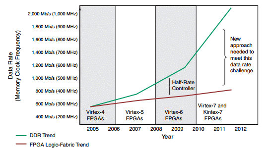
Now all you G’PU’ folks (As I hold my nose to you, ‘pu’) probably don’t care about such terms of DSP48s, or BRAMs but I do know that we all care about our very special DDR3/4 Memory. The memory technology as of today has addressed and solved many bandwidth issues but is just about past its prime. What is the problem you ask? Good question. The problem is IO. The term of the decade is Giga, you know a Billion. Silicon cannot keep the same IO footprint of DDR signaling to/from the memories. If you start to do the math and extrapolate out a bit you will see that the data the FPGA is consuming on a front end could not be buffered very deep no longer for future designs, even if you used a Virtex-8. What if for instance you were designing a RADAR front end and needed to buffer a whole CPI of data across 10,000 elements. Remember the FPGAs today have 28gb GT’s per lane!

Now the solution is not going to be 32 Banks of DD4 using 1200 LVDS, I wonder if the future of memory will be Gigabit IO instead of LVDS DDR. I think so, and when this happens it will open up not only the FPGA data processing pipes but unleash the CPU and GPUs as well. Now don’t say that is hard, everything about silicon is hard but the challenge needs to be overcome. Secondary to this memory design is the FPGAs ability to download an image from PROMs or FLASH so the FPGA can be configured. Xilinx FPGAs have the ability of partial reconfiguration which works well for designs such as software defined radio, but for RADAR applications it comes up short.
The issue is reprogramming times in the RADAR realm need to be under a millisecond. Using today’s programming rates; that is not happening but if you get the pencil and paper out you could easily design away a gigabit configuration PROM. That is the easy part; the hard part is getting the FPGA bit stream inside the FPGA to go thru the numerous states to configure quickly, including AES schemes. The payoff is creating for instance a Surveillance RADAR and Missile and Fire Control RADAR using the same COTs board. When a threat is detected, reprogram the RADAR to become a MFCR and finish the track and engagement out. Don’t think that’s possible, like everything give it time and money and we’ll see it soon enough.

lang: en_US


TSMC CoWoS versus Intel EMIB Semiconductor Packaging