The wreckage that is Apple’s stock is a surprise to many including yours truly but it appears to mark the beginnings of a transition period that will result in freeing the company from the demands of Wall St as it appeals to the broader population of mainsteam America. I call it the Ma Bell Strategy. Unlike Microsoft or Intel, Apple sustained itself for the first 25 years of its life by serving its small cadre of loyal fans who could be counted on to say: “I am with the band”. The hyper growth stage that commenced with the iPOD enticed Wall St. to enter the game and thus the manic-depressive nature of the Hedge Funds infected the outlook of the company. Out of this comes, no doubt, introspection and an alternative approach that can stabilize the company as it appeals to the generous spirit of America that is not tied to the money changers. Apple has the opportunity to be the successor to the AT&T that existed pre 1980s breakup. With an expected announcement of a larger dividend outlay, Apple will cement an intergenerational loyalty from Grandma to Grand kids for decades to come. What company wouldn’t want that as a long-term way to stabilize its business?
During the past 100 years there was only one company that was AT&T. It was a monopoly to be sure but it delivered great service and unbreakable phones. Underneath it all was a technical giant that hired the best and brightest engineers to not only advance communications technology but to invent the future with developments such as the transistor and UNIX operating system. On the outside though it was as American as Apple Pie (no pun intended).
Above the waterline, AT&T’s monopoly status as a provider of a daily necessity meant it was within reach of nearly all and if not, then Congress would pass laws requiring that telephone lines be strung to the remotest great plains town. To recreate AT&T in the middle of the 20th century would be out of question given the cost of building out the wired line infrastructure. To the average American, AT&T projected consistency and safety in its products and services. This was enhanced when the company followed through with years of delivering strong dividends that grew in time to the point it became a major income supplement to retirees. At times the dividend payments have reached as high as 7%, often exceeding that of Government Treasuries. Therefore, the tragedy of the AT&T breakup was in the homes of the retired who expected it to be around forever.
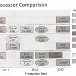
Apple is perceived to be in a tremendous battle with a host of mobile players who are looking to recreate the “Wintel” model that blunted the growth of the MAC in the 1990s. In reality, Apple and Samsung are taking home nearly 100% of the profits in an industry that has years of growth ahead of it. Within a year, both Apple and Samsung will complete filling out their smartphone and tablet product lines with LCDs sized from 4” to 11”. Then they ride down the component cost curve and ramp volume similar to how Dell did with PCs in the 1990s. Earnings should continue to expand nicely, especially if Apple is able to garner an edge in the corporate space. Assuming they upgrade iOS with multitasking capabilities, then there will be additional revenue from an “iPAD Pro” line that mirrors the way Microsoft sold its higher priced corporate O/S and Intel would sell high end processors. Value migration is still in play.
However, with all this being said, there is still the aspect of brand loyalty that is underrated but still determines the long term viability of a company and ensures stability in times of economic storms and product delays. This is ultimately where Tim Cook should aim to get to if he wants to spend more time building a company and less time responding to Wall St. demands and distractions. If he sets Apple on a course of a strong Dividend program then he will end up recruiting an army of well wishers, including Grandmas, across the entire spectrum of Red and Blue America that can counter the influence of Hedge Funds. It is well within his reach and it will be a good thing for the High Tech Industry.
Full Disclosure: I am Long AAPL, INTC, QCOM, ALTR