In 1990s when designs were small, I was seeing design and EDA community struggling to improve upon huge time taken to verify the circuits, specifically with Spice and the like. I was myself working on developing tool for transistor level static timing analysis (STA) mainly to gain on time (eliminating the need of exhaustive set of vectors to simulate) with acceptable loss of accuracy. That’s a history, but today, the challenge is much bigger and critical considering large memory blocks embedded in multi-million gate SoCs, and that too of varying types / functionalities, (e.g. SRAM, ROM, multi-port register etc.) with different modes of operations like on-demand active or stand-by mode. Moreover, the challenge has increased multi-fold with process variations at nano-meter level. Of course, there is gain on performance, power, area and cost reduction owing to economy of scale and that’s why it’s worth spending the effort. The need of the hour is to have better accuracy, faster verification and for larger designs – a triple whammy!
I was delighted to see Synopsys’s NanoTime tool which has transistor level STA engine well suited for today’s complex SoCs with multiple large instances of memory blocks embedded into them. That inspired me to go ahead and take a look at the white paper – The Benefits of Static Timing Analysis Based Memory Characterizationposted by Synopsys on its website – http://www.synopsys.com/Tools/Implementation/SignOff/Pages/NanoTime.aspx
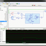
Synopsys provides novel approach to accurately estimate delays of sub-circuits within a memory block and use the graph analysis techniques to identify the most and least critical paths and determine all timing violations in a fraction of time taken by any dynamic circuit simulator.
The paths can extend from control logic through entire memory core to output buffers. The accuracy of result is again best within 5% of HSPICE. It supports both the approaches of memory model generation – characterization of memory compiler generated models and characterization of individual memory instances.
In the STA flow for memory design and characterization, the tool uses Spice/FastSpice as a sub-ordinate tool to further analyze and fine tune the timing violations found in the design at the first place.
Similarly memory compiler generated memory instances can also be characterized and verified by IP users.
It supports both timing models – Composite Current Source (CCS) and the standard Non-linier Delay Models (NLDM). The CCS model proposed by Synopsys for nano-meter delay modelling can be found at – http://www.opensourceliberty.org/ccspaper/ccs_timing_wp.pdf
The STA tool in NanoTime performs all types of timing checks pertaining to setup and hold times which are most crucial for the accuracy of sequential circuits. Several variants of these in the context of memory such as read / write time, read / write enable and so on; are all checked exhaustively and timing models are generated quickly for full-chip SoC sign-off. With all these kind of checks, it provides completeness on verification coverage as there are no vectors involved to be missed. It also checks Signal Integrity and does noise analysis. The tool has great capabilities in today’s context of designs.
By Pawan Kumar Fangaria
EDA/Semiconductor professional and Business consultant
Email:Pawan_fangaria@yahoo.com