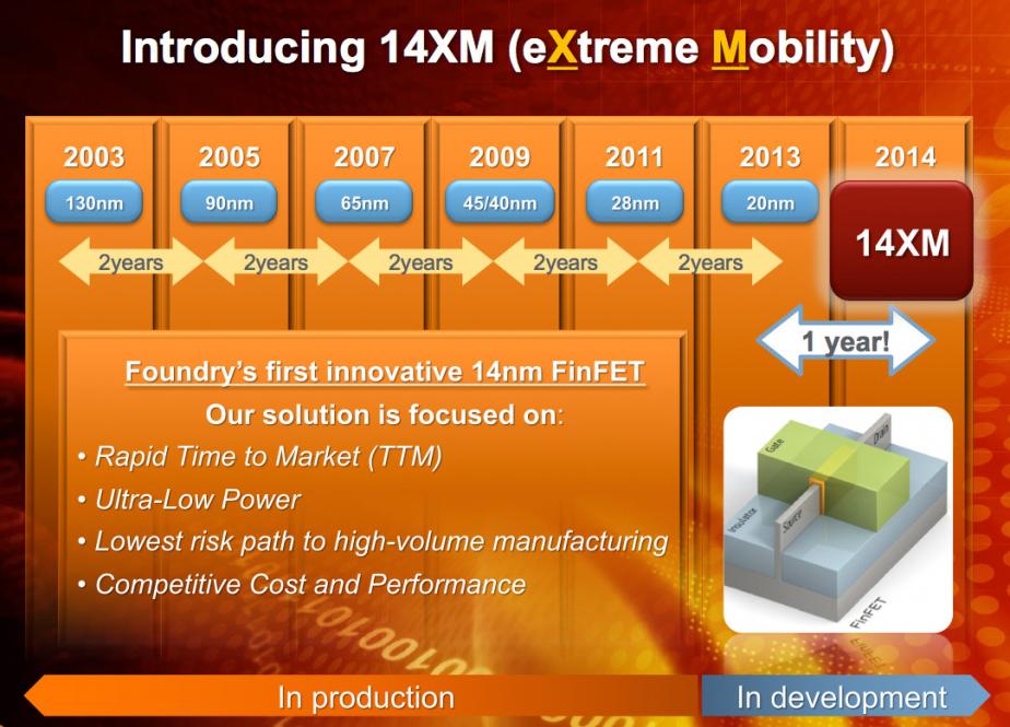


Today GlobalFoundries announced a 14nm process that will be available for volume production in 2014. They are explicitly trying to match Intel’s timeline for the introduction of 14nm. The process is called 14XM for eXtreme Mobility since it is especially focused on mobile. The process will be introduced just one year after 20nm, so an acceleration of about a year over the usual two year process node heartbeat.

The process is actually a hybrid, a low risk approach to getting (most of) the power and performance advantages of 14nm without a lot of the costs. The transistor is a 14nm FinFET but the middle-of-line and back-end-of-line are unchanged from 20nm, specifically 20nm-LPM process. So in effect it is 20nm process with 14nm transistors (at 20nm spacing). But this process gets a lot of the advantage of 14nm. It has 56% higher frequency at low operating voltages and 20% higher at high operating voltages. Or the voltage can be reduced by 160-200mV resulting in 40-60% increase in battery life.
Of course there is not really any area reduction from 20nm since all the metal pitches are the same. But it avoids the cost of having even more layers requiring double patterning and avoids needing to contemplate triple patterning. This is something I’ve been talking about recently, since there is a risk that future processes have higher performance and lower power but not lower cost. In the short term for existing high margin products like iPhone 5 this might not matter much, but in the long run it is the 1000 fold reductions in cost that drives electronics. If we hadn’t had that then we might still be able to make an iPhone in principle but it would cost as much as a 1995 mainframe of equivalent computing power.
GF have “fin-friendly migration” (FFM) design rules which they reckon should make migration planar designs, especially if they are already in the GF 20nm process that forms the basis for 14XM since only the transistors have changed.
Test silicon is being run in GlobalFoundries Fab 8 in upstate New York. Like other foundries, GF have been working on FinFETs for years even though they have none in a production process. Because the only thing that is new is the 14nm FinFet transistor, early process design kits are already available and customer product tape-outs are expected next year with volume production in 2014.
For more information on FinFETs (not specifically GlobalFoundries) here is my blog on a talk from Dr Chenmin Hu, the inventor of the FinFET. It explains the motivation for going away from planar transistors to FinFETs (or FDSOI, the only alternative technology that seems viable at present).


Consolidation and Competition: Who is Winning the $4.5 Billion Interface IP Race?