On Friday (April 19[SUP]th[/SUP]) I will be keynoting FinFET day at the EDPS conference in Monterey. This is an excellent opportunity to ask the experts about the challenges of FinFET design and manufacturing in an intimate setting (60 people). If you are interested register today and use the promo codeSemiWiki-EDPS-JFR and save $50.
Following the presentations there will be a panel discussion that I will describe in more detail in another blog. The panelists are from Qualcomm, ARM, and GLOBALFOUNDRIES with me moderating. Some very interesting questions will be asked and audience participation is a must.
A full program of the conference can be found HERE. I hope to see you there!
Here is how the day is organized:
Daniel NenniKeynote: The FinFET Value Proposition!
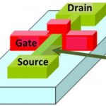
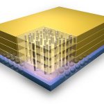
The most common theme amongst semiconductor ecosystem conferences this year is FinFETs. A lot has been written on SemiWiki.com about FinFETs, it is one of the top trending search terms, and probably the most exciting technology we will see this decade. The 1999 IDM paper “Sub 50-nm FinFET: PMOS” started the 3D transistor ball rolling then in May of 2011 Intel announced a production version of a 3D transistor (TriGate) technology at 22nm.
Intel is the leader in semiconductor process technologies so you could bet that the fabless semiconductor ecosystem would quickly follow, and we certainly have. Before we dive into the design and foundry challenges of FinFETs, I will set the stage with a brief history of the FinFET, where we are today in regards to FinFET process technology, and a look at the planar versus FinFET value proposition.
Tom Dillinger: FinFET Parasitic Extraction
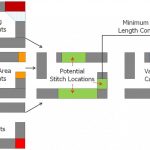
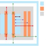
Parasitic extraction in a FinFET technology poses considerable complications, due to the unique topology of the vertical fin and of devices spanning multiple fins. Traditional methods for representing the parasitic gate input capacitances (Cgs, Cgd, and Cgx) will need to be adapted to the fin structure, as will the representation of the (equivalent) gate input resistance. The addition of dummy gates on the fin edges to improve uniformity also introduces unique parasitic modeling requirements. This presentation will briefly review the FinFET structure, and highlight the challenges with extracting a parasitic model.
Rob Aiken: Challenges of FinFET Design
The Challenges of FinFET Design FinFETs are the most significant innovation in SoC devices in decades. As a result, they affect the design process in many ways, but these are often more subtle than might be expected. For example, discrete device sizing presents challenges to circuit designers, but these can be largely hidden from higher level design. FinFET extraction, on the other hand, introduces changes that RTL designers will notice. This talk describes the challenges that will be observed throughout the SoC design process as a result of the migration to FinFETs, and shows how they can be addressed.
Raymond Leung:SRAM FinFET Design Challenges
Designing with FinFET technology presents many new challenges. This is further compounded by the introduction of new lithography steps such as double-patterning. This presentation will focus on SRAM FinFET design challenges and techniques used to deliver performance and power optimized SRAM at 14nm.
Tom Quan: FinFET Design Ecosystem Challenges
Semiconductor foundries must continuously push the technology envelope. With 28nm technology successfully up and running and the 20nm enters production in 2013, the design ecosystem continues to play crucial role in design enablement for FinFET process technology around the corner. Customers need to be able to bring their innovations to market through a comprehensive ecosystem that comprises both design enablement and design productization. TSMC is currently working with its design ecosystem partners to deliver complete 16nm FinFET design enablement including EDA tools, flows, and IP this year, followed by risk production by the end of 2013. Concurrent technology and design definition and development are required to deliver full design solutions to address FinFET design challenges at the device-, cell-, block- and chip-level. The ecosystem development phase, which orchestrates enablement activities so technology and design are ready at the same time.
To achieve this goal, design kits, reference foundation IP and design guidelines are provided to design partners. EDA and IP partners receive enablement kits tailored to their needs, which include pre-silicon certification and silicon validation for IP partners, and tool feature development and certification for EDA partners.
Finally, TSMC offers reference flows to help customers quickly ramp up new technology offerings, and scalable to the size and complexity of multicore systems-on-chip (SoCs).