
The second annual TSMC Open Integration Platform Ecosystem Forum was last week and let me tell you it was excellent. Great update on the TSMC process technology road maps, great for networking within the fabless semiconductor ecosystem, great for seeing what’s new in EDA and IP, and great for SemiWiki. It was time well spent for sure. You can see my TSMC OIP 2011 trip report HERE for reference.

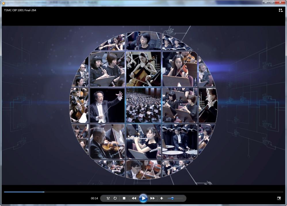
The opening video was excellent this year! It was all about collaboration of course and an orchestra is a perfect example. My wife played first chair violin so this theme really clicked with me. Last year’s theme was a rowing team which did not click with me. You can see the symphony videoHERE.
First up was Rick Cassidy. Rick is President of TSMC North America. Prior to joining TSMC in 1997 Rick was Vice President and General Manager of National Semiconductor’s Military and Aerospace Division. He joined National in 1979. Before that, Rick was an officer in the U.S. Army. He earned his Bachelor of Science degree from the United States Military Academy at West Point.
According to Rick attendance was up from last year which I certainly agree with. I counted 1008 seats in the main auditorium and estimate that 95% of them were taken. This does not include the partners manning the booths in the exhibition room next door.
Rick presented the TSMC vision and mentioned some interesting numbers:
*TSMC has more than 5,000 silicon validated IP available today, WOW! I have been through the TSMC silicon validation process many times and let me tell you it is rigorous to say the least.
*TSMC has invested $1.5B in design enablement thus far in 2012!
*TSMC in 1987 had one fab, a $20M CAPEX, 30 products and shipped 3,600 wafers
*TSMC in 2012 has 11 fabs, 5,498 different technologies, 12,569 products, $50B CAPEX, 615 customers, and a 15.3M wafer capacity!
Rick mentioned that his decision to join the semiconductor industry was based on the opportunity to change the world. I wish I could say the same. 30 years ago I was a starving college student and my decision was financial. I knew there was big money to be made in Silicon Valley and I wanted some. Looking back however we did change the world and there is still plenty of money to be made in doing so.
Next up was Dr. Mark Liu. Mark is TSMC’s Executive Vice President and Co-Chief Operating Officer. He joined TSMC in 1993 as an Engineering Manager. Prior to that Mark served in a number of technical capacities first with AT&T Bell Laboratories as a principal investigator in High Speed Electronics Research and later at Intel Corporation where he developed process technologies for Intel’s 32-bit microprocessors and flash memory products. Mark is a member of the Board of Directors of Silicon System Manufacturing Company in Singapore. He received Ph.D. degrees in electrical engineering and computer science from the University of California, Berkeley.
I met Mark when I toured Fab 12 in 2010, I blogged about it HERE. A memorable experience for sure. Mark ramped up TSMC’s first 200mm fab in 1993 and has been building fabs for TSMC ever since. Mark talked about “The Internet of Things” and what 2030 will look like. Mark also stated that:
*The TSMC 20nm design ecosystem (EDA and IP) are available today
*20nm is close to complete and will be in production next year
*TSMC will have three fabs for 20nm.
Next up was Dr. Cliff Hou, Cliff is vice president of R&D. Cliff’s door and mind is always open for new technology discussions and debates on the future of the semiconductor ecosystem. Cliff joined TSMC in 1997 and was appointed TSMC’s Vice President of Research and Development (R&D) in 2011. He was previously Senior Director of Design and Technology Platform where he established the company’s technology design kit and reference flow development organizations. He also led TSMC’s in-house IP development teams from 2008 to 2010. Cliff holds 20 U.S. patents and serves as a board member of Global Unichip Corp. He received his Ph.D. in electrical and computer engineering from Syracuse University.
Cliff added that:
*20nm engagements with partners and customers started much earlier
*TSMC overcame 20nm challenges through collaboration
*16nm FinFET will require even deeper collaboration
Cliff also mentioned that at 40nm partners and customers started design work when the PDK was release 0.5, at 28nm design work started at PDK 0.1, at 20nm design work started at PDK .05, and 16nm will start at PDK .01. The 20nm PDK 1.0 and 20nm foundation IP is silicon validated and available today with customer tape-outs expected in Q1 2013. 16nm PDK .1 will be available in Q1 2013 with the production version PDK 1.0 scheduled in Q4 2013.
The most interesting thing for me was the FinFET discussions and there were plenty of them which I will blog about separately. For those of you who don’t know about FinFETS start here with the FinFET Wiki. 2013 will be the year of the FinFET, absolutely!


Comments
0 Replies to “TSMC OIP Forum 2012 Trip Report!”
You must register or log in to view/post comments.