You are currently viewing SemiWiki as a guest which gives you limited access to the site. To view blog comments and experience other SemiWiki features you must be a registered member. Registration is fast, simple, and absolutely free so please, join our community today!
In the early days an IC had a single clock and a single reset signal, making it a simple matter to reset the chip into a known, stable state, so there was little need for detailed analysis. For modern designs there can be dozens to hundreds of clocks, creating separate domains and some use of asynchronous resets, so the challenge of ensuring proper reset logic has become quite complex. If the reset tree has any logic errors, like metastability, glitches or functional failures, then a costly design spin cycle ensues. I’ve read a white paper from Siemens on this topic and share my insights for this blog.
A Reset Domain Crossing (RDC) tool performs static verification to prevent unpredictable behavior, so it first analyzes RTL code to find all the reset logic, then classifies each reset:
Synchronous or asynchronous
Active high or low
Set or reset
Static analysis further identifies the type of reset tree and its control flow.
Origin of reset trees
Siemens proposes an advanced structural check for a thorough RDC verification.
RDC verification methodology
Consider the case where an asynchronous signal merges with a reset signal before reaching the register, signal FF1 may cause a glitch in the reset path.
An RDC path is flagged between register Tx and Rx, caused by signal combo_rst. Your design team then fixes the error by changing the reset domain to make it synchronous with the reset signal or by specifying a constant or a stable signal on the asynchronous signal.
Non-resettable registers (NRR) on asynchronous reset paths may lead to an RDC issue in the reset path of Rx:
Questa RDC has a reset integrity check that identifies logic on NRRs, then a design engineer fixes the metastability issue.
If an asynchronous reset signal Rst is also used as data then it will create an RDC error, so the designer will be alerted to fix their RTL code to avoid this type of logic. If you really want this logic, then add a waiver to Questa RDC.
Case Study
The Questa RDC tool was run on three designs of varying sizes and complexities to give you an idea of how the static analysis provides thorough feedback to RTL designers on basic and advanced reset tree issues.
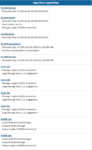
Design Complexity Comparisons
Structural issues were found in each of the three designs caused by basic reset tree issues.
There were a wide range of advanced reset tree issues identified by RDC validation.
Summary
The Questa RDC verification approach is quite thorough, ensuring the integrity of the reset tree logic, avoiding subtle errors caused by metastability, glitches and functional bugs. Both basic and advanced RDC verification are required, so that design teams can fix errors before tapeout, ensuring the most reliable and safe operation of a new chip. The earlier that you find these RTL issues, the more solid your design becomes and the quicker your team learns about best RDC practices.
Slava Libman, Ph.D. is the CEO of FTD solutions, the provider of facility management solutions that improve sustainability and enhance efficiency in industrial facilities. With more than 25 years of experience in water technology, Dr. Libman is a sought-after speaker and an active leader in the water and semiconductor industries. His contributions include more than 60 publications, conference organization, and presentations. He is actively involved in policy and climate technology related to ultra-pure water, water and wastewater treatment, desalination, filtration, reverse osmosis, biological wastewater treatment, and semiconductor water technology roadmap and standards.
Tell us about your company?
FTD solutions is the leading provider of digital twin technology supporting semiconductor industry sustainability. We deliver advanced, sustainable solutions for industries with complex water use demands. We optimize water efficiency, reuse, and recycling to help companies achieve significant resource savings and enhance their sustainability practices.
FTD solutions addresses environmental goals through digital transformation in industrial water management with a solution called the Water Management Application (WMA). With our Facility Management Application (FMA), in industrial facilities where the environmental footprint is significant, where water and energy conservation are valuable, and where greenhouse emission control is mission critical, we unlock sustainable processes that save money, energy, and more. Recently, we closed our Series A funding round with an investment from Ecolab.
What problems are you solving?
Many industrial processes require high water utilization, generate wastewater, and consume energy – the supply and costs for which are not sustainable in the long term. At the same time, complexity of the semiconductor facilities makes it difficult to optimize their performance without advanced information management tools and top level expertise. FTD solutions is solving these problems for industrial clients by saving water and energy while reducing carbon and greenhouse gasses – all with a strong return on investment. The FTD platform transforms water system data into actionable insights, enabling enterprises to standardize and enhance water conservation efforts, even across sites. The solution is supported by a patented algorithm and expert guidance. The WMA and FMA ensure compliance, optimize infrastructure, and significantly reduce water usage. These solutions deliver substantial cost savings.
What application areas are your strongest?
We have strong expertise in the semiconductor industry, but many other industries also benefit from FTD solutions. We serve the refinery, manufacturing, water, chemical, food and beverage, machining, and pharmaceutical industries as well.
Our strongest application areas include industrial water management, ultrapure water technology, closed-loop water systems, and advanced water recycling and reuse strategies. We are particularly adept in supporting manufacturing and industrial sectors that require precise water balancing and resource recovery, making water systems more resilient and cost-effective.
What keeps your customers up at night?
Our customers have persistent concerns regarding water, the availability of it, the processing of it before, during, and after their industrial processes. They are awake at night worrying about sustainable design and operation of their facilities, while supporting uninterrupted high yield manufacturing, meeting water use regulations, and managing costs associated with water treatment and disposal. Many also worry about operational risks from water scarcity and want to ensure they are using resources as efficiently as possible. Our solutions provide peace of mind by helping them address these concerns head-on.
What does the competitive landscape look like, and how do you differentiate?
FTD has a patented solution that is unlike any other in the marketplace. While the competitive landscape includes traditional water consultants, technology providers, and sustainability firms, none of these firms can provide the intelligence and clear opportunities for saving resources and money within their processes. The uniqueness of the FTD role is in integration of its capabilities into the customer processes, providing an extension to the internal expertise and enhancement to information management systems. FTD maintains an independent and objective view on defining best solutions for the site-specific customer needs, while FTD systems and processes are designed to be non-disruptive to the customer operation. As such, FTD solutions is differentiated because it combines deep industry expertise with a focus on sustainable, data-driven solutions that align with each client’s unique water demands and regulatory challenges. Our customized approach ensures clients receive practical, scalable strategies tailored to their specific goals.
What new features/technology are you working on?
With the investment from Ecolab, FTD solutions is accelerating the development of its software and support systems. This includes the enhancement of our digital twin technology which will enable greater optimization of operations and the reduction of facilities’ environmental footprint. These are designed to empower industries to achieve their sustainability goals more effectively. FTD works to drive significant impact within the industrial sector, helping to foster environmentally responsible practices and enhance operational efficiency.
How do customers normally engage with your company?
Customers initially engage with us through consultations, water audits, and system evaluations. We dissect the customer needs and proposed optimized solution strategies within business boundaries and priorities. We partner closely to understand customer processes, identify pain points, and deliver tailored recommendations which allow them to meet their goals. Our engagements often involve both hands-on support and continuous monitoring, ensuring customers can adapt to new challenges and achieve their long-term water sustainability objectives. Customers can also check out our website or follow us on LinkedIn!
At the risk of calling down the forecast universal opprobrium, I’m going to disagree with Dan’s take on the centrality of Intel.
I don’t agree that Intel is too big/important to fail or that the US can’t succeed in semiconductors without it. Reading the comments on SemiWiki, suggests I’m in a minority here, but far from alone. Perhaps it’s easier for me to say this, coming from the UK with our widespread tall poppy syndrome (anything big and successful is automatically suspect) and less emotionally invested in Intel.
Nothing here is intended as any criticism of Intel’s people. It just feels now like Intel is fighting forces which can be delayed, but not ultimately resisted. Caught in a pincer between the success of the fabless design model and the relative decline of the x86 business, it arguably can’t sustain leading edge manufacturing without both massive external support and becoming a commercial foundry. But is that what Intel really wants and can succeed at? Broad line customer service was never in their DNA. Why not just split off the foundry side and keep the product group?
In some ways I hope I’m wrong here. A lot of people are working very hard to try to right the ship at Intel, facing the possibly hardest challenge ever seen in the semiconductor business. Much as some of us disagreed with Pat Gelsinger’s IDM2.0 plan and sometimes loose talk, you had to admire his sheer guts and determination. He felt like the last link back to the real men (who always had fabs) of the 70s and 80s – perhaps the last of the IDM true believers. But that world is finally slipping out of view in the rearview mirror.
Companies come and go – they have lifecycles just like their products. The average lifespan of a US company is only 15 years (having dropped from 67 years in the 1920s). At some point, even Intel will wither away and we’ll continue on regardless. Perhaps even CMOS will go the way of TTL, NMOS (as used on the 8086 and 80186) and all those other technologies we barely remember now.
If the US feels in a mess today with all its eggs in the TSMC/Taiwan basket, it is one entirely of its own choosing. It’s tempting to assume here that the choices of US companies and governments over the last three decades were consciously made and that the defense of Taiwan was factored into the cost-benefit analysis of those choices. But apparently not …
So now we are asking Intel to bail out the US by providing a domestic commercial foundry business. Every bit as much as many hope for the opposite – that the US bail out Intel.
Intel built itself – at least over the past 40 years – largely as a high performance microprocessor company. We’re now asking it to become something quite different. Even if that’s possible, I’m not convinced that’s what Intel really wants to – or should – do. It may fit the narrative which demands that Intel serve some vital national security role and start operating as a far more customer service oriented foundry business serving a much wider range of customers and designs. But can you really convert an America’s Cup foiling catamaran into a not quite so fast, but more versatile monohull racing yacht which doesn’t drop off its foils and come to a halt in lighter winds? And in the middle of the race?
What really matters is that technology continues to advance. And from a US perspective, that it retains a leadership position and effective strategic independence in semiconductors (note: I think that’s tolerable from a Western, non-US perspective, since the rest of us have lived with it for around 60 years already).
If we’re demanding that the US have its own foundry company, why not start from a blank sheet? Instead of committing the cardinal engineering error of writing a solution (Intel) into the spec instead of a requirement (we want our own foundry), create a new company. After all, isn’t that what the US does best ? And give the US government a stake if it’s putting up funding – a real, financial stake and not one in micromanaging employment policies. Split the foundry completely off from Intel and get rid of the current conflict of interest with Intel’s product groups. Recall some lessons from the SIA about industry collaboration and pull in talent from other companies. What you end up with may be 80 or 90% from Intel, but it needs to be a fresh start.
It’s often argued that Intel’s product and design groups gain some unique advantage from having close collaboration with Intel’s fabs or that they wouldn’t be competitive without this link. That certainly held in the past, but is far from certain today. Some claim Intel’s design teams are world class and others that they aren’t. Looking from outside with no direct knowledge, it all seems rather confusing and contradictory. Yet we know that for over 40 years Intel have reliably designed and produced some of the most complex, fastest chips seen. We’ve also seen AMD survive and thrive moving from internal fabs to TSMC. So what are we worried about here?
If you think Intel foundry shouldn’t be split off, just remember this: the risk that Intel becomes a follower, second best in everything it does. Intel will be behind TSMC in foundry, nVidia in AI and arguably AMD in x86. Is that what we really want for Intel – to be everyone’s favourite second source?
By all means have a US national foundry champion. Just do it properly. And don’t call it Intel. Let the Intel product group focus and return to its historic excellence. Shoehorning today’s Intel into the IDM 2.0 model won’t help Intel survive. And it won’t ultimately help the US.
I may well be wrong. But however Intel’s future plays out, looking back in 10 or 20 years time, we’ll likely have forgotten today’s chaos and confusion and view the outcome as something that was never in doubt. As Kierkegaard observed, “Life can only be understood backwards; but it must be lived forwards”. Living forwards isn’t going to be easy for Intel for some time. But it can survive. Though perhaps only as separate product and foundry businesses, with only the first called Intel.
IEDM turned 70 last week. This was cause for much celebration in the form of special events. One such event was a special invited paper on Tuesday afternoon from Intel’s Tahir Ghani, or Mr. Transistor as he is known. Tahir has been driving innovation at Intel for a very long time. He is an eyewitness to the incredible impact of the Moore’s Law exponential and his work has made a measurable impact on the growth of that exponential.
Tahir treated the audience to a colorful perspective on how we’ve arrived at the current level of density and scaling. Pervasive AI will demand substantial improvement in energy efficiency going forward and Tahir took the opportunity to call the industry to action to address these and other challenges as we move toward a trillion-transistor system in package. Here are some of the comments from this invited talk at IDEM as Intel’s Mr. Transistor presents the incredible shrinking transistor – shattering perceived barriers and forging ahead.
About the Presenter
Dr. Tahir Ghani
Dr. Tahir Ghani is a senior fellow and director of process pathfinding in Intel’s Technology Research Group. Tahir has a 30-year career at Intel working on many innovations, including strained silicon, high-K metal gate devices, FinFETs, RibbonFETs, and backside power delivery (BSPD), among others. He has filed more than 1,000 patents over his career at Intel and was honored as Intel’s 2022 Inventor of the Year. He has the nickname of “Mr. Transistor” since he’s passionate about keeping Moore’s Law alive.
About the Talk
Besides IEDM turning 70 this year, Moore’s Law will turn 60 next year. Tahir used this milestone to discuss the innovation that has brought us here and what needs to done going forward to maintain Moore’s Law exponential innovation.
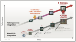
Tahir began by discussing a remarkable milestone that lies ahead – one trillion transistors within a package by the end of this decade. He took a sweeping view of the multiple waves of innovation that drove transistor scaling over the last six decades. The graphic at the top of this post presents a view of the journey, from system-on-chip to systems-in-package scaling. Tahir then presented the key innovations in this journey – past, present and future.
FIRST ERA: 1965 – 2005
The first four decades of Moore’s Law saw exponential growth in transistor count and enabled multiple eras of computing, starting with the mainframe and culminating in the PC. During this time, a second effect called Dennard scaling became important as well as Moore’s Law.
Robert H. Dennard co-authored a now-famous paper for the IEEE Journal of Solid State Circuits in 1974. Dennard and his colleagues observed that as transistors are reduced in size, their power density stays constant. This meant that the total chip power for a given area size stayed the same from process generation to process generation. Given the exponential scaling of transistor density predicted by Moore’s Law, this additional observation provided great promise for faster, cheaper and lower power devices.
Tahir explained that the happy marriage between Moore’s Law and Dennard scaling ushered in something he called the golden era of computing. The era was made possible by numerous innovations in materials and process engineering, most important being the consistent scaling of gate dielectric thickness (Tox) and the development of progressively shallower source/drain (S/D) extensions, which enabled scaling of gate lengths from micron-scale to nanometer-scale while lowering transistor threshold voltage (Vt).
From my point of view, these were the days when semiconductor innovation came from the process teams. If you could get to the next node, you’d have a faster, smaller and lower power product that would sell. Tahir explained that by 2005, power density challenges and the breakdown of Dennard scaling meant it was time for a new approach, which brings us to the present day.
SECOND ERA: 2005 – PRESENT
Tahir explain that during the last 20 years, technologists have shattered multiple seemingly insurmountable barriers to transistor scaling, including perceived limits to dimensional scaling, limits to transistor performance, and limits to Vdd reduction. This era marked the emergence of mobile computing, which shifted the focus of transistor development from raw performance (frequency) to maximizing performance within a fixed power envelope (performance-per-watt).
Many of the innovations from this era in materials and architectures came from Intel. In fact, Tahir has been in the middle of this work for many years. This work expedited the progress of groundbreaking ideas from research to development to high-volume manufacturing. Tahir explained that these innovations ushered in an era of astonishing progress in transistor technology over two decades. He discussed three important innovations from this time.
SEMINAL TRANSISTOR INNOVATIONS
Mobility enhancement leading to uniaxial strained silicon. In 2004, a novel transistor structure introduced by Intel at the 90nm node incorporated compressive strain for PMOS mobility enhancement. Intel’s uniaxial strain approach was in stark contrast to the biaxial strain approach pursued by the research community and turned out to be superior for performance and manufacturability. Moreover, this architecture proved scalable and enabled progressively higher strain and performance over the years.
Tox limit leading to Hi-K dielectrics and metal gate electrodes. Intel explored multiple approaches to introduce Hi-K gate dielectrics coupled with metal gate electrodes, including “gate-first,” “replacement-gate,” and even fully-silicided gate electrodes. The replacement metal gate flow adopted by Intel at the 45nm node in 2007 continues to be used in all advanced node processes to this day.
Planar transistor limits lead to FinFETs. The scaling of the planar transistor finally ran out of steam after five decades, mandating a move to the 3D FinFET
Fin profile improvements at Intel
structure. Intel was the first to introduce FinFETs into production at the 22nm node in 2011. Nanometer-scale fin widths enabled superior short-channel effects and, thus, higher performance at lower Vdd. The figure to the right illustrates the evolution of the fin profile over the last 15 years. The 3D structure of fins resulted in a sharp increase in effective transistor width (Zeff) within a given footprint, leading to vastly superior drive currents.
LOOKING AHEAD: THE NEXT DECADE
Tahir made the observation that the seventh decade of Moore’s Law coincides with the emergence of yet another computing era. He pointed out that AI will redefine computing and is already causing a tectonic shift in the enabling silicon platform from general-purpose processors (CPUs) to domain-specific accelerators (GPUs and ASICs).
Gate all around (GAA) transistor
He went on to say that this shift in computing platform also coincides with another inflection in transistor architecture. By completely wrapping the gate around the channel, the gate-all-around (GAA) transistor is poised to replace the FinFET. GAA transistors deliver enhanced drive current and/or lower capacitance within a given footprint, superior short-channel effects, and a higher packing density. The figure at the right shows what a GAA device looks like in silicon.
Looking ahead, he said the GAA architecture will likely be succeeded by a stacked GAA architecture with N/P transistors stacked upon each other to create more compact, monolithic 3D compute units. Looking further ahead, he explained that 2D transition metal chalcogenide (TMD) films are being investigated as channel material for further Leff scaling, but many issues are still to be addressed.
CALL TO ACTION: NEW TRANSISTOR
Tahir concluded his talk with a sobering observation- worldwide energy demand for AI computing is increasing at an unsustainable pace. Transitioning to chiplet-based system-in-package (SiP) designs with 3D stacked chips and hundreds of billions of transistors per package will increase heat dissipation beyond the limits of current best-in-class materials and architectures. Breaking through this impending “Energy Wall” will require coordinated and focused research toward reducing transistor energy consumption and improving heat removal capability. A focused effort is necessary to develop a new transistor capable of operating at ultra-low Vdd (< 300mV) to improve energy efficiency.
He went on to point out that ultra-low Vdd operation can lead to significant performance loss and increased sensitivity to variability, requiring circuit and system solutions to be more resilient to variation and noise. This suggests the need for a strong collaboration between the device, circuit, and system communities to achieve this important goal. There are many ways to attack this problem.
Tahir reviewed a few, including Tunnel FET (TFET), Negative Capacitance FET (NC-FET), and Ferroelectric FET (FE-FET). All have significant obstacles to overcome. New materials and new structures will need to be explored.
Conclusion
Dr. Tahir Ghani covered a lot of ground in this exceptional review of past, present and future challenges for semiconductor scaling. The best way to end this discussion is with an inspirational quote from Tahir.
“At every significant inflection in the past, when challenges to continued transistor scaling seemed too daunting, technologists across industry and academia forged new paths to enable the arc of exponential progress to continue unabated. There is no reason to believe that this trend will not continue well into the future. There is still plenty of room at the bottom.”
Tahir recently did a Semiconductor Insider’s podcast on SemiWiki. You can hear some of his views in this compelling discussion here. And that’s how Intel’s Mr. Transistor presents the incredible shrinking transistor – shattering perceived barriers and forging ahead.
A crucial step in helping any new technology specification gain adoption is certification. NIST has been hard at work establishing more than post-quantum cryptography algorithms – they’ve also integrated the new algorithms into their process for third-party validation testing to ensure implementations are as advertised. Secure-IC is the first security IP and software vendor to achieve official worldwide NIST algorithm certification for post-quantum cryptography (PQC) software and secure element IP. Here’s a brief look at what NIST certification entails and what Secure-IC achieved.
An overview of NIST certification for crypto algorithms
NIST created its Cryptographic Algorithm Validation Program (CAVP) in 1995 to test FIPS-approved, NIST-recommended algorithms. Testing occurs on an Automated Cryptographic Validation Test System (ACVTS) with a NIST-controlled hardware environment. NIST offers a Demo ACVTS server as a sandbox environment and a Production ACVTS server accessible only by accredited third-party cryptographic and security testing (CTS) laboratories. Only tests by third-party CTS labs on the Production ACVTS server can advance as evidence for obtaining a CAVP certificate.
ACVTS spans capabilities for supported algorithms, including parameters such as message length, and automatically generates test cases and vectors for robust coverage. Vectors are suitable for feeding an implementation candidate, which can run its functions and provide outputs back to ACVTS. A correctness score for each algorithm in a test session returns. This approach keeps ACVTS testing as black-box – NIST never sees implementations as they are not uploaded to the ACVTS server, with only vectors sent and outputs returned.
NIST keeps the CAVP suite current, retiring outdated algorithms and incorporating new advancements as they become approved. CAVP online documentation contains a current list of algorithms and their specifications, validation testing requirements, validation lists, and test vectors.
Moving from PQC algorithms to crypto module certification
PQC algorithms are now part of the CAVP suite, and validation testing of PQC implementations can ensue. Since we last discussed PQC here, some of its algorithms received less informal, more technically accurate names from NIST. CRYSTALS-Kyber is now known as ML-KEM (module-lattice-based key-encapsulation mechanism), and CRYSTALS-Dilithium now goes by ML-DSA (module-lattice-based digital signature algorithm).
Secure-IC conferred with an in-country CTS-accredited lab, SERMA Safety and Security, to validate its Securyzr™neo-product for PQC. A summary of the algorithm tests appears in the NIST validation certificate, A6046, dated October 30, 2024. Secure-IC focuses on optimizing its implementations for fast throughput in SoC-optimized IP blocks ready for hardware design.
CAVP validation is crucial because compliance is ultimately a function of the complete system context for an implementation, as with many specifications. CAVP is a mandatory prerequisite for certifying a cryptographic module, a combination of hardware and software in an end product. NIST also shepherds a Cryptographic Module Validation Program (CMVP), transitioning from FIPS 140-2 compliance to FIPS 140-3, reflecting the recommendation for PQC implementations. A full FIPS 140-2 sunset date of September 2026 incentivizes module designers to get moving with their CMVP validation. Any system requiring cryptographic protection must conform to FIPS 140-3 requirements – with PQC incorporated – by that date.
Secure-IC is committed to helping its customers navigate these requirements and quickly bringing PQC into the mainstream. Their PQC-enabled solutions are configurable and scalable to meet a range of cryptography needs, with an eye on performance and power efficiency. Their achievement of certification for post-quantum cryptography algorithms puts their customers ahead in the race for protecting platforms from advanced cybersecurity threats. More information is available in a press release from Secure-IC, which includes more details on the Securyzr neo-product certification, links to the official NIST certificate, and background on the cooperation with SERMA Safety and Security.
Dan is joined by Nilesh Kamdar, the General Manager of the Design & Verification EDA businesses at Keysight. Nilesh has also held roles as Portfolio Manager, and Director of the Software Business & Operations team at Keysight. Nilesh joined Hewlett-Packard in 1999 in the EEsof EDA division. Over his 25+ year career he has worked in various leadership roles including leading the Learning Products team, Circuit Simulation and Architecture team, and the Application Engineering and Customer Success team.
Dan explores the structure, focus and impact of the Keysight Design & Verification EDA business with Nilesh. This high-growth portion of the company focuses on high frequency, high speed designs. Nilesh explores the challenges design teams face. Multi-chip design is growing for this segment and there are many new challenges. He explains how Keysight takes a multi-physics approach to address chip/package/system requirements.
Keysight also builds high-performance chips for its test & measurement products in its own fab so the company has first-hand experience addressing the challenges its customers face. Nilesh also explores the impact AI will have on the design process in detail, as well as the benefits of the company’s engineering lifecycle management tools.
The views, thoughts, and opinions expressed in these podcasts belong solely to the speaker, and not to the speaker’s employer, organization, committee or any other group or individual.
Caroline Guillaume is the Chief Executive Officer of TrustInSoft. She has an extensive background working in the critical software industry, notably at Thales Digital Identity and Security where for 14 years she contributed to the Sales division including as the VP of Sales – Software Monetization Europe and VP of Banking and Telecom Solutions Sales out of Singapore. She also previously worked as director of Product Marketing at Gemplus. Caroline holds an engineering degree from Télécom SudParis.
Tell us about your company?
TrustInSoft is a leader in advanced software analysis tools and services that specializes in formal verification of C and C++ source code to ensure safety, security and reliability. Recognized by the US National Institute of Standards and Technology (NIST) for leveraging advanced formal methods, including abstract interpretation, TrustInSoft can mathematically guarantee analyzed software is free of critical runtime errors and vulnerabilities. TrustInSoft serves a diverse range of industries including automotive, aerospace, defense, consumer electronics, and IoT industries.
What problems are you solving?
The problem we’re tackling is one that’s plagued software development since its inception – bugs, vulnerabilities, and unexpected failures. These issues can have devastating consequences, leading to security breaches, system crashes, and even physical harm in critical industries. More than that, TrustInSoft’s tools and services help you find the very subtle and critical bugs that often go unseen and have costly consequences on the field.
For developers and testers, TrustInSoft Analyzer provides exhaustive static analysis with up to zero false positives and no false negatives. Our customers have seen up to 40X less time spent detecting bugs and 4X decrease in verification time. This helps answer to problems like tight time-to-market constraints and software safety, security, and reliability.
What application areas are your strongest?
Our technology can benefit many applications from the most critical like defense, aeronautics, and EVs, to consumer devices, and telecommunications. We intervene in the low-level software and ensure safety, security, and reliability by securing the foundation of critical systems.
The tool performs a combination of static analysis based on formal methods. Static analysis allows us to exhaustively test code without actually running it, identifying potential problems before they ever cause an issue. Formal methods take it a step further – they provide a mathematical guarantee that the code is free of certain types of errors, specifically undefined behaviors.
What keeps your customers up at night?
Notably in critical software and modern IoT devices, software developers and testers might lay awake wondering if they’ve done all they can to safeguard their code from hackers and corner cases. We help give them peace of mind by taking an incremental approach to secure their test suites, exhaustively fuzz the code, and even provide formal mathematical proof that the software will behave as specified. We combat undefined behaviors which can lead to software defeat, security breaches, challenges for regulatory compliance, and tight time to market requirements without sacrificing quality and security.
What does the competitive landscape look like and how do you differentiate?
TrustInSoft Analyzer, is not your average static analysis tool. Our use of formal methods gives a guarantee of safety, security, and reliability by identifying all undefined behaviors, which are amongst some of the top CWE list vulnerabilities. TrustInSoft Analyzer guarantees zero false negatives and up to zero false positives, saving precious developer and tester time and effort.
What new features/technology are you working on?
We are constantly improving TrustInSoft Analyzer with two major updates per year. This October’s release includes:
Streamlined and Intuitive User Experience: The enhanced TISA UI dramatically simplifies the analysis process, making complex software verification more accessible and reducing the learning curve for technical teams
Enhance Your Accuracy and Efficiency with TrustInSoft Assistant Capabilities: advanced assistant capabilities guide users in setting up and tuning their analysis, ensuring accurate results and reducing the risk of errors in complex environments.
Advanced Compliance and Performance Capabilities: new features, including CWE alarm mapping, ARINC support, and enhanced C++ analysis performance, enable technical teams to achieve higher compliance and efficiency in complex environments.
How do customers normally engage with your company?
Our customers typically either use our tool, TrustInSoft Analyzer, independently or combine their tool usage with our Formal Verification Services (FVS). We help secure everything from airplanes to consumer devices like smartphones and gaming systems at the embedded systems layer ensuring safety and cybersecurity earlier in the development cycle. Our team of experts helps integrate into existing verification and validation processes to help developers dig into the vulnerabilities in their code.
The main program for the 70th IEDM opened on Monday morning in San Francisco with an excellent keynote from Dr. Yuh-Jier Mii, Executive Vice President and Co-Chief Operating Officer at TSMC. Dr. Mii joined TSMC in 1994. Since then, he has contributed to the development and manufacturing of advanced CMOS technologies in both fab operations and R&D. In 2022, he received the IEEE Frederik Philips Award recognizing his outstanding accomplishments in the management of research and development. He holds 34 patents globally, including 25 US patents, and holds a B.S. in electrical engineering from National Taiwan University, as well as an M.S. and Ph.D. in Electrical Engineering from the University of California, Los Angeles (UCLA). He treated the audience to a broad view of technology innovation in his keynote. Let’s look at how IEDM opens with a big picture keynote from TSMC’s Yuh-Jier Mii.
About IEDM
To begin, that wasn’t a typo above. The 70th annual IEEE International Electron Devices Meeting (IEDM) just concluded. This incredibly long-lived conference began tracking technology innovation in the vacuum tube era. For seven decades the event has tracked semiconductor and electronic device technology, design, manufacturing, physics, and modeling. This year’s event had a record high number of submissions at 763 and a record number of accepted papers at 274.
The figure below summarizes the growth of this premier conference over the years.
2024 IEDM paper statistics
About the Keynote
Dr. Yuh-Jier Mii
Dr. Mii began his keynote with a short but compelling video that provided an overview of some of the innovations that have occurred in the semiconductor industry in general, and some of the advances contributed by TSMC in particular. All of this is driving the development of a trillion-transistor system in the near future. These trends are summarized in the graphic at the top of this post.
Dr. Mii touched on five key areas in his talk. I will provide a summary of his remarks. He began with a semiconductor industry & market outlook (I). AI is poised to play a key role in the industry’s growth as we move toward one trillion dollars in revenue by 2030. He projected that high-performance computing will contribute 40% of this number, mobile 30%, automotive 15%, and IoT 10%. He discussed the how ubiquitous AI technology is becoming across many products and markets. Generative AI and large language models are contributing to this growth and the complexity of the models for these new applications and the associated training required present substantial new challenges.
He pointed out that these new applications will require gigawatts of power within a few years. Reducing power consumption will be critical to allow these applications to flourish and new device technology and architectural advances will be needed.
Next, Dr. Mii discussed advanced logic technologies (II). He described the industry’s move from planar devices to FinFETs and most recently nanosheet technology for gate-all-around devices at 2nm. Patterning also advanced from immersion lithography to EUV and multi-patterning EUV. Design technology co-optimization, or DTCO has also helped to bring technology to new levels. For example, backside power delivery has helped to reduce power and increase density.
Regarding logic technology frontiers (III), Dr. Mii discussed the evolution from FinFET to nanosheet FET to vertically stacked complimentary or CFET architectures. He explained that the CFET approach holds great promise to allow continued Moore’s Law scaling with its 1.5 – 2X density improvement when compared to nanosheet devices. He described the work going on at TSMC to make CFETs a reality. At this year’s IEDM, TSMC is presenting the first and smallest CFET inverter at a 48nm pitch.
Dr. Mii explained that beyond CFET, the ongoing quest for higher performance and more energy-efficient logic technologies necessitates an accelerated search for channel materials that go beyond those based on silicon. He explained that carbon nanotubes (CNTs) and transition metal dichalcogenides (TMDs) have garnered significant interest due to both their physical and electronic properties. In the area of interconnects, he discussed a new 2D material that is being explored as a superior alternative to copper. This material shows lower thin film resistivity than copper at reduced thicknesses, helping to mitigate line resistance increases in scaled geometries and enhance overall performance.
Dr. Mii then moved to a discussion of system integration technologies (IV). While pushing 2D technology scaling to enable better transistors and higher packing density in monolithically integrated SoCs is important, so are innovations beyond the chip level to extend integration into the heterogenous domain.
He explained that advanced silicon stacking and packaging technologies, including SoIC, InFO, and CoWoS® continue to aggressively scale down the chip-to-chip interconnect pitch, offering the potential to improve 3D interconnect density by another six orders of magnitude. These trends are summarized in the figure below.
Advanced silicon stacking and packaging technologies
Dr. Mii discussed an emerging System-on-Wafer (SoW) technology, where all the chiplets and HBM memories for an entire system can be integrated directly on a 12-inch wafer. He explained that this approach can deliver an additional 40X compute improvement when compared to the most advanced data center AI accelerator today. Optical interconnect was also discussed, which can provide 20X more power efficiency than copper interconnect. Vertical stacking of logic and optical transceivers will help deliver these improvements. He explained that today the laser light source is outside the chip, but efforts are underway to integrate the laser on chip as well.
Dr. Mii concluded with a discussion of specialty technologies (V). Many of the items discussed here are high frequency or analog in nature to accommodate the interface between the digital and analog (real) world. He discussed innovations spanning N16 to N4 to accommodate the increased demands of new standards for WiFi.
Advances in embedded non-volatile RAM were also discussed in this part of the keynote. The benefits and challenges of both MRAM and RRAM were covered. CMOS image sensors were also discussed. This is a critical technology for automotive applications. As pixel size decreases, new approaches are needed to maintain sensitivity and dynamic range. Dr. Mii described work to separate the photo diode from the pixel device and re-integrate them using 3D wafer-to-wafer stacking.
Summary
Dr. Mii concluded by observing that semiconductor innovations, encompassing advances in device technology, system-level scaling, and customer-specific design ecosystems will remain pivotal in driving rapid technological progress in the era of AI. He pointed out that TSMC is actively exploring a new array of innovations for future generations of technology, system integration platforms, and design ecosystems. These efforts will be crucial in meeting the increasing societal demands for energy-efficient, data-intensive computing in the coming decades. He invited the audience to join in this important collaboration. And that’s how IEDM opens with a big picture keynote from TSMC’s Yuh-Jier Mii.
The December 2024 WSTS forecast called for strong 2024 semiconductor market growth of 19%. However, the strength is limited to a few product lines. Memory is projected to grow 81% in 2024. Logic is expected to grow 16.9%. The micro product line should show only 3.9% growth, while discretes, optoelectronics, sensors and analog are all projected to decline. If the memory product line is excluded, the WSTS forecast for the rest of the semiconductor market in 2024 is only 5.8%.
The strength of memory in 2024 is also reflected in semiconductor company revenues. Revenue for the first three quarters of 2024 compared to a year earlier show gains of 109% for both Samsung Memory and SK Hynix. Micron Technology is up 78% and Kioxia is up 54%. The strongest growth among major semiconductor companies is from Nvidia, up 135%. Nvidia strength is due to its AI processors. Nvidia’s revenues also include memory purchases, adding to its revenue.
The robust memory growth is largely driven by memories for AI applications. Prices for memory have increased in 2024, especially for DRAM. Trend Force estimated average DRAM prices will be up 53% in 2024. Thus, one application, AI, is accounting for most of the growth of the semiconductor market in 2024. The revenues for the first three quarters of 2024 compared to the same three quarters of 2023 show a 97% gain for memory companies and a 135% gain for Nvidia. The total semiconductor market was up 19.9% for this period. Excluding the memory companies, the remainder of the semiconductor market was up only 6.8%. If both the memory companies and Nvidia are excluded, the rest of the semiconductor market declined 10.5%
Several major semiconductor companies experienced revenue declines in 1Q 2024 through 3Q 2024 versus a year earlier. STMicroelectronics and Analog Devices were each down 24%. Texas Instruments, Infineon Technologies, NXP Semiconductors, and Renesas Electronics also declined. These companies largely depend on the automotive and industrial sectors, which have been weak in 2024. Companies heavily dependent on the smartphone market showed revenue increases, with Qualcomm’s IC business up 10% and MediaTek up 25%. Among computer dependent companies, Intel was flat, and AMD was up 10%. Broadcom counts on AI for a significant portion of its revenues. Its calendar 3Q results have not yet been released, but it should be up about 47%.
Thus, except for AI and memory, the semiconductor market has been weak in 2024. Our Semiconductor Intelligence forecast of 6% growth in the semiconductor market in 2025 assumes some strengthening of core markets of PCs, smartphones, automotive and industrial. The rapid growth rates of memory and AI in 2024 should be significantly lower in 2025.
Memory has long exacerbated the cycles of the semiconductor industry. The chart below shows annual change in the semiconductor market based on WSTS data through 2023 and the WSTS forecast for 2024. Total semiconductor is compared with memory and semiconductor excluding memory. While the memory market has shown extremes of 102% growth and a 49% decline, the market excluding memory has been somewhat more stable, ranging from plus 42% to minus 26%. In the last ten years, the memory market change has ranged from plus 81% in 2024 to minus 33% in 2023 while the market excluding memory has ranged from plus 25% to minus 2%.
Over the last forty years, whenever the memory market has grown over 50%, it has seen a significant deceleration or a decline in the following year. In the six times this has occurred prior to 2024, the memory market has declined in the following year four times. In two cases the market has seen positive but significantly slower growth the following year and declines two years after the peak. These trends are driven by basic supply and demand for a commodity product. Memory prices and production rise when supply is below demand. When supply is above demand, production and prices fall. Thus, we should expect a significant downturn in the memory market either in 2025 or 2026.
Semiconductor Intelligence is a consulting firm providing market analysis, market insights and company analysis for anyone involved in the semiconductor industry – manufacturers, designers, foundries, suppliers, users or investors. Please contact me if you would like further information.
Bill Jewell
Semiconductor Intelligence, LLC
billjewell@sc-iq.com
Mikko Utriainen – Founder – Chief Executive Officer, Feng Gao – Founder – Chief Technology Officer, Pasi Hyttinen – Founder – Chief Data Officer
Tell us about your company? Chipmetrics is a Finnish company specializing in metrology solutions for high aspect ratio 3D chips, especially 3D NAND and 3D DRAM with an eye on GAAFET and CFET structures. We are a young but mature company founded in 2019 with over 40 customers worldwide, and we’re looking to further scale up our international business efforts in the coming years.
This far, in addition to our home market in northern Europe, we’ve found success in Japan and we’re also represented in other key markets such as South Korea, Taiwan and USA.
What problems are you solving? We provide test chips that enable companies to develop next-generation 3D semiconductors, speeding up associated R&D and process control workflows with quick access to high-quality data.
With our various test chips, engineers can check the quality of their film deposits with an ellipsometer or other conventional surface analysis tools near-instantaneously, rather than sending them away for analysis which can take weeks. This gives access to high-quality data quickly, which in its turn cuts down on development time of 3D chips.
What application areas are your strongest? We have a unique position in metrology solutions for film deposition, be it ALD or CVD. Considering that ALD was originally invented in Finland, it feels extra special to be able to offer Finnish solutions as ALD technology is becoming more and more relevant with 3D semiconductors.
What keeps your customers up at night? Challenges with conformal deposition, gap-fill deposition and selective deposition, the latter especially in DRAM. High-quality films and quality control are also at the forefront of our clients’ minds. As ever, they also wish to speed up their time to market and lower the process temperatures.
What does the competitive landscape look like and how do you differentiate? We believe we have a unique niche with our test chips and metrology solutions. That said, we do jack into the ALD landscape with batch systems, where our test structures are needed.
What we do with our PillarHall family of test chips is speed up process control screening without diminishing accuracy. It is, to our knowledge, the only practical way to measure film quality, properties, microstructure, the elemental composition of the sidewall in a high aspect ratio cavity on a wafer level.
What new features/technology are you working on? This summer, we launched the latest iteration of the PillarHall, LHAR5. It allows for metrology of high-aspect ratio chips with gap heights as low as 100 nanometers. At the same time, we launched the ASD-1 chip, for Area Selective Deposition, in our quest to offer a complete lineup of 3D metrology chips.
We also value collaboration with our clients, meaning we’re busy ideating and iterating with them and coming up with custom concepts and test structure wafers for them.
How do customers normally engage with your company? We have well defined products for sale. Interested parties can easily approach us with a short RFQ email through our website and we reply fast. Our clients are typically recurring with orders, and we believe they come back in part due to our high service level. Also our product development is based on the repeat order customer feedback and needs. We are also active in digital marketing, trade shows and scientific conferences. Those are important forums for startups in the semiconductor field, and for us especially the AVS and SEMI events have been useful. Lastly, the core Chipmetrics team consists of industry veterans with strong personal networks that we tap into, and on top of this we have local representatives in key markets.