Chris Rowen of Cadence’s Tensilica announced the tenth generation of the Xtensa customizable processor at the Linley Microprocessor Conference yesterday. Chris was one of the founders of Tensilica…back in 1997. I believe that the first version was released in 1999. Over the years the Tensilica business changed. Originally they sold the Xtensa system to customers to build their own customized processors, and a few customers still do that today. But most customers had a problem to solve and many had the same problems. So Tensilica used the Xtensa system to build processor environments specifically for those problems: HiFi Audio, LTE modems, video processing and so on, with software stacks, codecs and anything else needed. But still retaining the capability to customize the processor further. Delivering more value tends to be a good business strategy and with a couple of billion cores out there and an acquisition by Cadence at a healthy multiple, it turned out to be.
Now they are onto the tenth generation. The problems have changed a lot over time. Well, mainly the performance requirements have only gotten higher and higher but the power budgets have…not. Tensilica’s processors are often used to offload the control processor in various applications, or to create systems with performance that cannot be approached with a general purpose processor. Terabit data rates for example. Usually the big motivation is power: offload the application processor in a smartphone to play mp3 at much lower power, or design an LTE modem without requiring a power hungry multicore general purpose processor. Back in 1997 we didn’t worry much about power.
Another thing we didn’t worry so much about back then was programmability for its own sake. We had a specification, we wrote RTL and we taped out the chip. But now designs have to be more flexible since often the chip design has to be frozen before the specification is finalized. Being first to market often means starting the design earliest. In many environments new standards or tweaks to the standard show up. The only way to make that sort of late change is for it to be in software. But a general purpose processor is much too power hungry and, often, too low performance to do the job. The sweet spot is a processor that is optimized for the job in hand but is still programmable to take account of late changes and new standards.
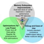
So what is new? I am not going to attempt to list everything or this blog would be unreadably long. There is obviously a lot of focus on power. There is a lot of dynamic clock gating. This is similar to the sequential clock gating that tools from several EDA vendors provide, except that the Xtensa system knows much better which values will be used, and in many cases this cannot be deduced from static analysis of the RTL since it is concealed in the software. A lot of unnecessary memory access can be avoided this way.
Talking of memory, there are a lot of memory subsystem improvements to improve bandwidth and to increase parallelism. This allows for a wider range of programming models.
There is a small (up to 256 bytes) L0 cache. It would seem that would be almost useless. Funnily enough one of the first computers I ever programmed was the Cambridge University Titan system. They added a 32 word cache (so about the same size) indexed off the lowest 5 bits of the PC. Again, it seems like it wouldn’t make much difference. But it can make a big difference since it ensures that any loop of less than 32 instructions runs out of cache. And algorithms often have a lot of small tight inner loops with just a few instructions. For example, mp3 decode spends 40% of its time in this sort of loop.
In summary:
- Less core and system power
- More data throughput
- Lower latency
- More flexible memory hierarchy for more flexible programming models
- Maximum visibility and control for rapid system development and optimization