llmda newsletter ad (2)

My iPhone 5s is having hot flashes!

My iPhone 5s is having hot flashes!
by Daniel Nenni on 11-29-2013 at 1:53 pm

It is bad enough my wife is “flashing” but now my phone is 100+ degrees too!?!?!? It seems that an application is getting stuck and the SoC is thrashing. Which application I do not know, you need to use the old process of elimination method to figure this one out. Doing a hard reboot (turning your phone off and on) is the quick fix, you can also restart your phone using factory settings. But I ask Apple here and now what is REALLY going on?
I switched from my beloved Blackberry to the iPhone 4s 2+ years ago and couldn’t be happier. My personal and professional productivity has increased exponentially, absolutely. My wife and kids all have iPhones and we are a much tighter family unit as a result. Relationships are all about communication right? So to the hard working people at Apple I say, “Thank you for inventing the smartphone and I’m really looking forward to the iPhone 6 with a blazing fast TSMC 20nm SoC.”

Unfortunately battery life is a real concern and as we see more integration of features into the SoC and more applications on our phones, applications that get “stuck” are going to be a deafening problem! After Googling around I have found that this is not just an Apple problem, Samsung phones are burning up too so spare me the Apple bashing.Back in the day there were a dozen or so chips on a computer mother board. In fact, when I first started working at Data General a CPU consisted of multiple printed circuit boards. Now if you look at the latest SoC from QCOM just about everything our phone does is on one chip. You would think having less chips in your phone would extend battery life but they also added more cool features so it seems to be a wash. No matter what phone I have I get about a day’s worth of use unless of course an application gets stuck then it is a matter of minutes. And don’t tell me your phone is better because you get more than a day’s use because I use mine way more than you do.

Battery life is now part of the mainstream benchmarking process, which is good, but as I have written before, benchmark cheating is the second oldest profession so I really don’t trust any of them. In fact, Samsung was just caught benchmark cheating yet again by multiple benchmarking sites. Do you see a pattern here? Apparently Samsung has some low level code that detects when you run a benchmark and it reconfigures to get better results. So go ahead and brag about how good your Samsung phone or tablet is or how much market share they now have knowing full well that the company itself is ethically bankrupt.

One final comment, for those of you who think your fingerprint will end up in a NSA database from the new sensor on the iPhone 5s thank you for the laugh out loud. Just wait for Google glasses to do a retina scan on you.

More Articles by Daniel Nenni…..

lang: en_US


Intel’s Tale of Two Cities

Intel’s Tale of Two Cities
by Ed McKernan on 11-27-2013 at 11:00 pm

It was a year ago that Paul Otellini made his surprise announcement that he was stepping down as CEO of Intel. Soon after, I wrote an article asserting that the only correct choice for his replacement was Nvidia’s CEO Jen Hsun Huang. I went beck to reread what I wroteand I can scarcely say I would change anything I put in the article assuming Intel intends to continue down the path of trying to win mobile with Atom and limiting the Foundry prospects to non-compete fabless players like Cisco and Altera. Andy Bryant’s confession of missing the tablet market aside, the company though moves closer to a split due to financial gravity that is trying to shake Intel’s Board and Executives to the reality that the Fabs are more valuable than mobile Atom where x86 is valued at next to nil.

Intel is evolving into two companies and now the Fab side of the house represented by Andy Bryant and newly minted CEO Brian Krzanich have the reigns. They know that the company is still well funded with the awesome Data Center Group and traditional x86 PC client group that has been able to execute a slow retreat by aggressively moving into the higher ASP ultrabook market, where AMD and nVidia do not play well for cost, space and power reasons. Intel charges a premium with its ULV processors, but this may not last over the long run as mobile processors are undercutting the premium by as much as several hundred dollars. The other side is the Foundry that demands $11B of capex each year to keep them running with bigger bills on the 450mm horizon. Mobile atom is the worst of times in the famous Dickens novel. It is on track to lose $2.4B on $4B in sales this year.

At first the analyst cheered at the news that Intel would quadruple tablet processor sales in 2014 to 40MU. Then the cheers changed in tune to what one might hear in the Bronx when the home team fails as CFO Stacey Smith announced revenue would be flat in 2014. Digging deeper, one sees that to sell 40M processors requires quite a bit of marketing dollars. Intel doesn’t discount processors, they instead offer an ad campaign to get the word out that Intel Inside is now alive inside mobiles. Analysts are not thrilled when there is no light at the end of the tunnel to Intel’s mobile adventures.

If Intel were to split, I would still place my money on Jen Hsun Huang as the true Andy Grove heir that could make sense of what to build from servers to mobiles with the optimum mix of processor, graphics and communications. Selecting Jen Hsun would create a monopoly in the data center and close off all competitors to a piece of business that may be larger than the PC x86 group in 5 years time. Alas, it will probably not come to fruition, unless Intel enters more dire straits and the board is replaced with folks who want not just change but strong growth.

It is not hard for someone of Jen Hsun’s experience to see that tablet has split irreconcilably and that the corporate windows piece can and should be supported by a trimmed down version of Intel’s Broadwell processor while consumer is tailing away with ARM as the best low cost solution. With a sea of solutions, branding and simplicity still count as valuable to buyers who care, both corporate and consumer. Everyone looks for a company to trust.

The irony of Intel’s dilemma is that for many years they espoused the beauty of the PC’s horizontal market with each slice providing unique value. If you doubt, go read Andy Grove’s “Only the Paranoid Survive.” Paul Otellini, in his final two years would exclaim to Wall St, that Intel liked to get paid twice for its intellectual property, the first for the foundry and the second for the x86 architecture. It appears this is not so in the mobile space and truly it is not x86 that determines the second stack value but all that legacy software that needs to run as is.

Today Mr. Market clearly is saying that the Foundry must take its independent horizontal slice and create value separate from Xeon and Core x86 processors. The high castle walls that protect Xeon and Core are not transferrable to mobile, where ARM started out with an enormous lead and where Apple has virtually declared that custom processors will be forever closely coupled to iOS. Why not build for them and fill a fab or two at the expense of rapidly gaining rivals Samsung and TSMC.

Waiting for Intel to split the company is not what most investors envisioned and it may turn into a long drawn out game until someone like a Carl Icahn comes in and forces the hands of the board. Who will be CEO at the split is anyone’s guess but to at one moment in the Analyst Meeting proclaim that the Foundry is open to all and the next minute discuss how great mobile Atom is going to be for Intel’s future is to essentially mean that the great trigate process is beholden to the smallest part of the business that may start bleeding not a trickle but a flood if 40MU are sent to wayward homes.

lang: en_US

More articles by Ed McKernan…


Lithography: Future Technologies

Lithography: Future Technologies
by Paul McLellan on 11-27-2013 at 12:28 pm

The first part of Lars Liebmann’s ICCAD keynote about lithography was on the changes in lithography that have to us to where we are today. In some ways it was an explanation of why we have the odd design rules, double patterning etc that we have in 20nm and 16nm processes. The second part of his talk was a look forward to how we might be able to go further.

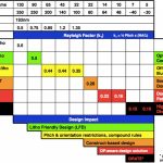
Once again, here is the Rosetta Stone of Lithography, a summary of how lithography affects EDA at each process node all in one table.

The first approach that we can use down to 7nm is pitch multiplication. For some layers at earlier process nodes we need to use self-aligned double patterning (SADP) or sidewall image transfer (SIT). But we can use this technique twice to get quadruple patterning. This is known as self-aligned quadruple patterning (SAQP) or as SIT[SUP]2[/SUP]. The basic idea is that a mandrel is put down, as with SADP, and the sidewalls are deposited and the mandrel removed. But now we do it again, and use those original sidewalls as new mandrels, and deposite sidewalls on the sidewalls and remove the original sidewalls/mandrel. This gives us a grating at 4 times the pitch we can achieve with the basic optical (which is 80nm). Theoretically this would be 20nm but in practice is is more like 30nm.

The second approach is directed self assembly (DSA). I’ve written about this before. The basic idea is to take two polymers that won’t mix like oil and water. If they are just deposited on the wafer then you get a random pattern a bit like a fingerprint. However, if some guide layout is already in place, then the polymers line up in a neat tight grid that can then be divided up with a cut mask. It is resolution in a bottle. A few years ago this was a novelty that looked unlikely to be of any practical relevance, but with increasing investment and experiments it is starting to look increasingly practical.

The third approach, that I have also written extensively about, is extreme-ultra-violet (EUV). This is using 14nm light (versus 193nm that we have been using for the last decade). There are a lot of challenges with EUV but here are the ones I think are the most significant:

  • intensity of the light source. EUV is generated by zapping droplets of molten tin with a huge laser. But currently the intensity of the light is not enough to get a wafer throughput that is high enough to be economically competitive
  • EUV is absorbed by everything including lenses and air. So the entire system needs to be in a vacuum and we need to go to reflective optics, not refractive. In fact normal mirrors also absorb EUV so we need mirrors that are made up of layers of silicon and molybdenum. These reflect about 30% of the incident EUV so only about 2% of the EUV generated at the source makes it to the photoresist on the wafer
  • EUV masks have defects. It is impossible to see the defects until the multiple layers of the mirror are constructed and then it is too late. But the bottom line is that it is not possible to guarantee that masks are defect free
  • There is no pellicle on an EUV (reflective) mask since it would absorb the EUV. So unlike in refractive optics, any contamination on the mask will be in the focal plane and will print


The big challenge going forward is that increasingly it looks like we will only be able to lay down regular gratings and then use a cut mask to divide them up. The big question is whether that is good enough for us to be able to design the kind of structures that we need on the silicon. The big problem layer is first metal since it is very difficult to design standard cells with first level metal being unidirectional. There is local interconnect (which is contactless and just connects to everything it crossed) but there are lots of challenges, especially in power delivery.


More articles by Paul McLellan…


eMMC Mobile Memory

eMMC Mobile Memory
by Paul McLellan on 11-27-2013 at 11:40 am

eMMC is the standard for mobile memory used in smartphones and tablets. The latest standard, released just this year, is eMMC 5.0. The previous standard, 4.51, was only released last year so things are moving quickly.

Arasan have a webinar next week to bring you up to speed on eMMC 5.0 in general and, of course, their own IP offering in the space in particular. It is at 6pm on Tuesday evening December 3rd (convenient both for the west coast of the US and also for Asia).

The new standard, as you would expect, supports higher bandwidth at 3.2Gbps. See the table below for other changes between the two standards.

[TABLE] class=”cms_table_grid” style=”width: 500px”
|- class=”cms_table_grid_tr”
| class=”cms_table_grid_td” |
| class=”cms_table_grid_td” | eMMC 4.51

| class=”cms_table_grid_td” | eMMC 5.0

|- class=”cms_table_grid_tr”
| class=”cms_table_grid_td” | Throughput

| class=”cms_table_grid_td” | 1.6Gbps
| class=”cms_table_grid_td” | 3.2Gbps
|- class=”cms_table_grid_tr”
| class=”cms_table_grid_td” | Pins

| class=”cms_table_grid_td” | 10 pins
| class=”cms_table_grid_td” | 11 pins
|- class=”cms_table_grid_tr”
| class=”cms_table_grid_td” | I/O voltages

| class=”cms_table_grid_td” | 1.2V/1.8V/3.3V
| class=”cms_table_grid_td” | 1.2V/1.8V
|- class=”cms_table_grid_tr”
| class=”cms_table_grid_td” | Data bus width

| class=”cms_table_grid_td” | 4 or 8 bit
| class=”cms_table_grid_td” | 8 bit
|- class=”cms_table_grid_tr”
| class=”cms_table_grid_td” | Clock

| class=”cms_table_grid_td” | 200 MHz (SDR)
| class=”cms_table_grid_td” | 200 MHz (DDR)
|-

One other big difference is that eMMC 5.0 has a hard IP analog PHY, including DLLs for Tx, Rx and Rx STRB. This standard is expected to be widely used. IHS iSuppli predict shipments of almost a billion units by 2015.

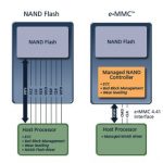
So just what is eMMC? It is a full managed flash memory solution, including features such as bad block management, error detection and correction and NAND flash wear leveling. The previous version of the standard is already widely used in most smartphones and tablets. It is a complete memory subsystem including both hardware and software.


One challenge with new standards is that there are no devices available using the standard because it is so new. So a hardware validation platform is required that functions as an eMMC 5.0 host to enable early validation and software development. This consists of a standard PC motherboard along with an eMMC 5.0 host IP board build using FPGA technology.


Arasan is the only company with eMMC 5.0 IP shipping. It is available now in TSMC 28nm, both HPM and LP (high performance and low power variants of the process) and is silicon proven. The IP is delivered as:

  • NV-DDR2 PHY in GDSII
  • Controller IP core in RTL along with timing and behavioral models
  • Software stack in C++ for Linux
  • Available hardware validation platform

Once again the Arasan webinar is next Tuesday, December 3rd, at 6pm Pacific. Registration is here.


More articles by Paul McLellan…


Intel Bay Trail Fail II

Intel Bay Trail Fail II
by Daniel Nenni on 11-27-2013 at 9:00 am

To follow up my Bay Trail Fail blog which predicted that the leading edge Intel 22nm mobile SoC offering would fail, I must admit I was wrong. I did not think Bay Trail would see any traction in the tablet market but, as it turns out, Intel will ship 40M of those parts in 2014. Did you notice I said ship and not sell? Read on………
Continue reading “Intel Bay Trail Fail II”


Social Media at ARM

Social Media at ARM
by Daniel Payne on 11-26-2013 at 3:27 pm

The number one semiconductor IP company in the world is ARM, and they have really figured out how to use social media in a big way to communicate with and listen to their customers. When you first visit the Home page for ARM there are four social media icons displayed in monochrome underneath the menu bar. As you hover over the icons (Twitter, Facebook, YouTube, Google+) you see a color version light up.
Continue reading “Social Media at ARM”


What’s new in the “Interface IP Survey” ?

What’s new in the “Interface IP Survey” ?
by Eric Esteve on 11-26-2013 at 9:27 am

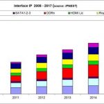
The reader will find many updates in the “Interface IP Survey” from IPNEST, released in October 2013. Good question, as the IP market is a very fast moving one and the protocol based Interface IP, is moving even faster… exhibiting 20% growth rate in 2012, expected to grow with 10% CAGR between 2012 and 2017 to reach $700M.

Continue reading “What’s new in the “Interface IP Survey” ?”


Semiconductor Process Development: A View from the Trenches at IEDM

Semiconductor Process Development: A View from the Trenches at IEDM
by Daniel Nenni on 11-25-2013 at 10:00 pm

There is always a lot of posturing and pontificating when semiconductor executives talk about the future of process development. They are fighting an air war of perception and investor expectations, so naturally want to make sure they have plenty to brag about. But, as we pointed out recently with Intel’s problems at 14nm, moving from one generation to the next is not easy – and it’s only getting harder.

So what do the guys who are really hands on when it comes to process development – the developers at the big IDMs, the memory providers and the foundries — think about the challenges facing them with the current and next generation of process technology? Are we really nearing the end of Moore’s Law? Can we get past 14nm and 10nm and into single digit geometries?

At IEDM, our friends at Coventor have assembled an impressive line-up of folks to give you perhaps another point of view. First, let me say that IEDM is a great event and brings together world class thinkers – and doers – to talk about device manufacturing. This year’s event is December 7-10 in Washington DC.

Coventor is hosting a reception that promises to be more than just free drinks and hotel finger food. They’ve invited 6 heavy hitters who get their hands dirty every day worrying about how to move process technology along. Plus, their own CTO of Semiconductor, David Fried – who can hold his own with anyone when it comes to talk of FinFETS, 3D ICs, flash memory and other challenging IC manufacturing topics – will be in the mix as well (David runs the group within Coventor that develops the SEMulator 3D virtual fabrication software platform that many manufacturers are using to reduce the time and effort required to develop new processes).

Joining David will be Dr. Brian Green from IBM; Mark Fisher from Micron; Dr. Andy Wei from GLOBALFOUNDRIES; Jaouen Herve from ST Microelectronics; Sean Lian from Samsung; and Laith Altimime from IMEC.

If you want to hear what’s really going on in the world of process development, you won’t find a better place. These guys are ready to talk openly and honestly, so you can expect some great insights.

The Coventor-sponsored event will be held on:
Tuesday, December 10 at theChurchill Embassy Row Hotel (Kalorama West room). The hotel is right across the street from the Washington Hilton where IEDM is held. Doors open at 5:30PM and the discussion begins at 6:30PM.
To RSVP for the event, drop an email to RSVP-to-COVENTOR@coventor.com

About Coventor
Coventor, Inc. is the market leader in automated design solutions for micro-electromechanical systems (MEMS) and virtual fabrication of MEMS and semiconductor devices. Coventor serves a worldwide customer base of integrated device manufacturers, fabless design houses, independent foundries, and R&D organizations that develop MEMS-based products for automotive, aerospace, industrial, defense, and consumer electronics applications, including smart phones, tablets, and gaming systems. Coventor’s software tools and expertise enable its customers to simulate and optimize MEMS device designs and fabrication processes before committing to time-consuming and costly build-and-test cycles. More information is available at http://www.coventor.com.

About IEDM

With a history stretching back nearly 60 years, the IEEE International Electron Devices Meeting (IEDM) is the world’s pre-eminent forum for reporting technological breakthroughs in the areas of semiconductor and electronic device technology, design, manufacturing, physics, and modeling. IEDM is the flagship conference for nanometer-scale CMOS transistor technology, advanced memory, displays, sensors, MEMS devices, novel quantum and nano-scale devices and phenomenology, optoelectronics, devices for power and energy harvesting, high-speed devices, as well as process technology and device modeling and simulation. The conference scope not only encompasses devices in silicon, compound and organic semiconductors, but also in emerging material systems. IEDM is truly an international conference, with strong representation from speakers from around the globe.

lang: en_US


Front-End Design Summit: Physically Aware Design

Front-End Design Summit: Physically Aware Design
by Daniel Nenni on 11-24-2013 at 12:00 pm

Save closure time and boost performance by incorporating knowledge of physically aware design early into your front-end design implementation flow

With the adoption of advanced process nodes, design closure is becoming increasingly difficult due to the lack of convergence between the front end and the back end of the register-transfer level (RTL)-to-signoff flow. Incorporating knowledge of physically aware design early in the front-end design process is quickly becoming a must-have to enable faster convergence in the back end.

Join us at the Front-End Design Summit, where you can network with fellow logic designers and speak directly with Cadence® R&D experts from our Encounter® RTL Compiler, Encounter® Test, and Conformal® product teams. At this day-long technical event, you will:

  • Hear from Cadence customers the challenges they faced during logic synthesis, advanced low-power design and verification, engineering change order (ECO), and design-for-test (DFT) implementation, and the strategies they employed to address them
  • Discover how best to achieve power, performance, and area goals on industry-leading IP cores
  • Network, share your knowledge, and exchange best practices with your industry peers
  • Hear from Cadence R&D on product updates, solutions, and future directions
Win an Apple Mini iPad®! Drawing will be held at the end of the event.


Date: 05 Dec 2013 (9:00am – 5:00pm PST)
Location:Cadence Design Systems Campus, Bldg. 10 , San Jose, CA

Agenda
[TABLE] cellpadding=”5″ style=”border-bottom: #ccc 1px solid; border-left: #ccc 1px solid; margin-top: 5px; border-collapse: collapse; border-top: #ccc 1px solid; border-right: #ccc 1px solid”
|-
| valign=”top” style=”border-bottom: #ccc 1px solid; border-left: #ccc 1px solid; border-collapse: collapse; background: #eee; border-top: #ccc 1px solid; border-right: #ccc 1px solid” | Time
| valign=”top” style=”border-bottom: #ccc 1px solid; border-left: #ccc 1px solid; border-collapse: collapse; background: #eee; border-top: #ccc 1px solid; border-right: #ccc 1px solid” | Title
| valign=”top” style=”border-bottom: #ccc 1px solid; border-left: #ccc 1px solid; border-collapse: collapse; background: #eee; border-top: #ccc 1px solid; border-right: #ccc 1px solid” | Speaker
|-
| valign=”top” style=”border-bottom: #ccc 1px solid; border-left: #ccc 1px solid; border-collapse: collapse; border-top: #ccc 1px solid; border-right: #ccc 1px solid” | 9:00am
| valign=”top” style=”border-bottom: #ccc 1px solid; border-left: #ccc 1px solid; border-collapse: collapse; border-top: #ccc 1px solid; border-right: #ccc 1px solid” | Registration and Breakfast
| valign=”top” style=”border-bottom: #ccc 1px solid; border-left: #ccc 1px solid; border-collapse: collapse; border-top: #ccc 1px solid; border-right: #ccc 1px solid” |
|-
| valign=”top” style=”border-bottom: #ccc 1px solid; border-left: #ccc 1px solid; border-collapse: collapse; border-top: #ccc 1px solid; border-right: #ccc 1px solid” | 9:30am
| valign=”top” style=”border-bottom: #ccc 1px solid; border-left: #ccc 1px solid; border-collapse: collapse; border-top: #ccc 1px solid; border-right: #ccc 1px solid” | Welcome
| valign=”top” style=”border-bottom: #ccc 1px solid; border-left: #ccc 1px solid; border-collapse: collapse; border-top: #ccc 1px solid; border-right: #ccc 1px solid” | Andy Lin, VP of R&D, Front End Design, Cadence
|-
| valign=”top” style=”border-bottom: #ccc 1px solid; border-left: #ccc 1px solid; border-collapse: collapse; border-top: #ccc 1px solid; border-right: #ccc 1px solid” | 9:45am
| valign=”top” style=”border-bottom: #ccc 1px solid; border-left: #ccc 1px solid; border-collapse: collapse; border-top: #ccc 1px solid; border-right: #ccc 1px solid” | Keynote
| valign=”top” style=”border-bottom: #ccc 1px solid; border-left: #ccc 1px solid; border-collapse: collapse; border-top: #ccc 1px solid; border-right: #ccc 1px solid” |
|-
| valign=”top” style=”border-bottom: #ccc 1px solid; border-left: #ccc 1px solid; border-collapse: collapse; border-top: #ccc 1px solid; border-right: #ccc 1px solid” | 10:15am
| valign=”top” style=”border-bottom: #ccc 1px solid; border-left: #ccc 1px solid; border-collapse: collapse; border-top: #ccc 1px solid; border-right: #ccc 1px solid” | Advantages of RTL Compiler Using Physically Aware Structuring
| valign=”top” style=”border-bottom: #ccc 1px solid; border-left: #ccc 1px solid; border-collapse: collapse; border-top: #ccc 1px solid; border-right: #ccc 1px solid” | Jaga Shanmugavadivelu, Techincal Lead, Cisco Systems
|-
| valign=”top” style=”border-bottom: #ccc 1px solid; border-left: #ccc 1px solid; border-collapse: collapse; border-top: #ccc 1px solid; border-right: #ccc 1px solid” | 10:45am
| valign=”top” style=”border-bottom: #ccc 1px solid; border-left: #ccc 1px solid; border-collapse: collapse; border-top: #ccc 1px solid; border-right: #ccc 1px solid” | Break
| valign=”top” style=”border-bottom: #ccc 1px solid; border-left: #ccc 1px solid; border-collapse: collapse; border-top: #ccc 1px solid; border-right: #ccc 1px solid” |
|-
| valign=”top” style=”border-bottom: #ccc 1px solid; border-left: #ccc 1px solid; border-collapse: collapse; border-top: #ccc 1px solid; border-right: #ccc 1px solid” | 11:00am
| valign=”top” style=”border-bottom: #ccc 1px solid; border-left: #ccc 1px solid; border-collapse: collapse; border-top: #ccc 1px solid; border-right: #ccc 1px solid” | Addressing Physical Challenges Early in RTL Synthesis
| valign=”top” style=”border-bottom: #ccc 1px solid; border-left: #ccc 1px solid; border-collapse: collapse; border-top: #ccc 1px solid; border-right: #ccc 1px solid” | Ankush Sood, R&D Director, Cadence
|-
| valign=”top” style=”border-bottom: #ccc 1px solid; border-left: #ccc 1px solid; border-collapse: collapse; border-top: #ccc 1px solid; border-right: #ccc 1px solid” | 11:30am
| valign=”top” style=”border-bottom: #ccc 1px solid; border-left: #ccc 1px solid; border-collapse: collapse; border-top: #ccc 1px solid; border-right: #ccc 1px solid” | ECO Experience on a High Performance Mobile ASIC
| valign=”top” style=”border-bottom: #ccc 1px solid; border-left: #ccc 1px solid; border-collapse: collapse; border-top: #ccc 1px solid; border-right: #ccc 1px solid” | Deepa Thali, Staff Engineer, Qualcomm
|-
| valign=”top” style=”border-bottom: #ccc 1px solid; border-left: #ccc 1px solid; border-collapse: collapse; border-top: #ccc 1px solid; border-right: #ccc 1px solid” | 12:00pm
| valign=”top” style=”border-bottom: #ccc 1px solid; border-left: #ccc 1px solid; border-collapse: collapse; border-top: #ccc 1px solid; border-right: #ccc 1px solid” | Corporate Update
| valign=”top” style=”border-bottom: #ccc 1px solid; border-left: #ccc 1px solid; border-collapse: collapse; border-top: #ccc 1px solid; border-right: #ccc 1px solid” | Chi-Ping Hsu, Sr. VP R&D, DSG and CSO, Cadence
|-
| valign=”top” style=”border-bottom: #ccc 1px solid; border-left: #ccc 1px solid; border-collapse: collapse; border-top: #ccc 1px solid; border-right: #ccc 1px solid” | 12:15pm
| valign=”top” style=”border-bottom: #ccc 1px solid; border-left: #ccc 1px solid; border-collapse: collapse; border-top: #ccc 1px solid; border-right: #ccc 1px solid” | Lunch with R&D
| valign=”top” style=”border-bottom: #ccc 1px solid; border-left: #ccc 1px solid; border-collapse: collapse; border-top: #ccc 1px solid; border-right: #ccc 1px solid” |
|-
| valign=”top” style=”border-bottom: #ccc 1px solid; border-left: #ccc 1px solid; border-collapse: collapse; border-top: #ccc 1px solid; border-right: #ccc 1px solid” | 1:15pm
| valign=”top” style=”border-bottom: #ccc 1px solid; border-left: #ccc 1px solid; border-collapse: collapse; border-top: #ccc 1px solid; border-right: #ccc 1px solid” | Optimizing PPA for Tensilica BBE32 Core
| valign=”top” style=”border-bottom: #ccc 1px solid; border-left: #ccc 1px solid; border-collapse: collapse; border-top: #ccc 1px solid; border-right: #ccc 1px solid” | Jagesh Sanghavi, Engg. Director, Cadence
|-
| valign=”top” style=”border-bottom: #ccc 1px solid; border-left: #ccc 1px solid; border-collapse: collapse; border-top: #ccc 1px solid; border-right: #ccc 1px solid” | 1:45pm
| valign=”top” style=”border-bottom: #ccc 1px solid; border-left: #ccc 1px solid; border-collapse: collapse; border-top: #ccc 1px solid; border-right: #ccc 1px solid” | Power-Efficient SmartScan Test Architecture for Processor Designs
| valign=”top” style=”border-bottom: #ccc 1px solid; border-left: #ccc 1px solid; border-collapse: collapse; border-top: #ccc 1px solid; border-right: #ccc 1px solid” | Alan Hales, DFT Lead, Texas Instruments
|-
| valign=”top” style=”border-bottom: #ccc 1px solid; border-left: #ccc 1px solid; border-collapse: collapse; border-top: #ccc 1px solid; border-right: #ccc 1px solid” | 2:15pm
| valign=”top” style=”border-bottom: #ccc 1px solid; border-left: #ccc 1px solid; border-collapse: collapse; border-top: #ccc 1px solid; border-right: #ccc 1px solid” | Addressing Test Challenges for GigaScale SoCs
| valign=”top” style=”border-bottom: #ccc 1px solid; border-left: #ccc 1px solid; border-collapse: collapse; border-top: #ccc 1px solid; border-right: #ccc 1px solid” | Michael Vachon, Group Director R&D, Cadence
|-
| valign=”top” style=”border-bottom: #ccc 1px solid; border-left: #ccc 1px solid; border-collapse: collapse; border-top: #ccc 1px solid; border-right: #ccc 1px solid” | 2:45pm
| valign=”top” style=”border-bottom: #ccc 1px solid; border-left: #ccc 1px solid; border-collapse: collapse; border-top: #ccc 1px solid; border-right: #ccc 1px solid” | Break
| valign=”top” style=”border-bottom: #ccc 1px solid; border-left: #ccc 1px solid; border-collapse: collapse; border-top: #ccc 1px solid; border-right: #ccc 1px solid” |
|-
| valign=”top” style=”border-bottom: #ccc 1px solid; border-left: #ccc 1px solid; border-collapse: collapse; border-top: #ccc 1px solid; border-right: #ccc 1px solid” | 3:00pm
| valign=”top” style=”border-bottom: #ccc 1px solid; border-left: #ccc 1px solid; border-collapse: collapse; border-top: #ccc 1px solid; border-right: #ccc 1px solid” | Comparison of Various Flows for Post-Mask ECO: Manual vs. Conformal-ECO
| valign=”top” style=”border-bottom: #ccc 1px solid; border-left: #ccc 1px solid; border-collapse: collapse; border-top: #ccc 1px solid; border-right: #ccc 1px solid” | Pihay Saelieo, Senior MTS CAD Design Engineer, Spansion
|-
| valign=”top” style=”border-bottom: #ccc 1px solid; border-left: #ccc 1px solid; border-collapse: collapse; border-top: #ccc 1px solid; border-right: #ccc 1px solid” | 3:30pm
| valign=”top” style=”border-bottom: #ccc 1px solid; border-left: #ccc 1px solid; border-collapse: collapse; border-top: #ccc 1px solid; border-right: #ccc 1px solid” | Streamlining Your Verification Flow
| valign=”top” style=”border-bottom: #ccc 1px solid; border-left: #ccc 1px solid; border-collapse: collapse; border-top: #ccc 1px solid; border-right: #ccc 1px solid” | Kei-Yong Khoo, Group Director R&D, Cadence
|-
| valign=”top” style=”border-bottom: #ccc 1px solid; border-left: #ccc 1px solid; border-collapse: collapse; border-top: #ccc 1px solid; border-right: #ccc 1px solid” | 4:00pm
| valign=”top” style=”border-bottom: #ccc 1px solid; border-left: #ccc 1px solid; border-collapse: collapse; border-top: #ccc 1px solid; border-right: #ccc 1px solid” | Bridging the Gap in an RTL2GSDII Flow
| valign=”top” style=”border-bottom: #ccc 1px solid; border-left: #ccc 1px solid; border-collapse: collapse; border-top: #ccc 1px solid; border-right: #ccc 1px solid” | Paul Cunningham, VP of R&D, ICD, Cadence
|-
| valign=”top” style=”border-bottom: #ccc 1px solid; border-left: #ccc 1px solid; border-collapse: collapse; border-top: #ccc 1px solid; border-right: #ccc 1px solid” | 4:30pm
| valign=”top” style=”border-bottom: #ccc 1px solid; border-left: #ccc 1px solid; border-collapse: collapse; border-top: #ccc 1px solid; border-right: #ccc 1px solid” | Final Q&A and Conference Survey
| valign=”top” style=”border-bottom: #ccc 1px solid; border-left: #ccc 1px solid; border-collapse: collapse; border-top: #ccc 1px solid; border-right: #ccc 1px solid” |
|-
| valign=”top” style=”border-bottom: #ccc 1px solid; border-left: #ccc 1px solid; border-collapse: collapse; border-top: #ccc 1px solid; border-right: #ccc 1px solid” | 4:45pm
| valign=”top” style=”border-bottom: #ccc 1px solid; border-left: #ccc 1px solid; border-collapse: collapse; border-top: #ccc 1px solid; border-right: #ccc 1px solid” | Networking Event, iPad Mini Drawing
| valign=”top” style=”border-bottom: #ccc 1px solid; border-left: #ccc 1px solid; border-collapse: collapse; border-top: #ccc 1px solid; border-right: #ccc 1px solid” |
|-

Questions About this Event? Send email to events@cadence.com

Register »

lang: en_US