RVN! 26 Banner revised (800 x 100 px) (600 x 100 px)

Intel is Killing the Environment!

Intel is Killing the Environment!
by Daniel Nenni on 10-31-2013 at 6:00 pm

If I had to sum up opening day at ARM TechCon 2013 in one word it would be “crowded”. More than twice as many people attended as last year with 6,500 preregistered. The opening keynote was “The New Style of IT” pimping the HP Moonshot systems, but it could have just as easily been called “Why Intel Stock is Dead Money”, just my sarcastic opinion of course.

“It’s an exciting time to be in technology. The IT industry is at a major inflection point driven by four generation-defining trends: the cloud, social, Big Data, and mobile. These trends are forever changing how consumers and businesses communicate, collaborate, and access information. And to accommodate these changes, enterprises, governments and fast growing companies desperately need a “New Style of IT.” Shaping the future of IT starts with a radically different approach to how we think about compute – for example, in servers, HP has a game-changing new category that requires 80% less space, uses 89% less energy, costs 77% less – and is 97% less complex. There’s never been a better time to be part of the ecosystem and usher in the next-generation of innovation.”

The traditional Intel (cash cow) server market is now being challenged by more environmentally friendly microservers, low-power servers tailored towards tasks that require bandwidth versus raw compute power such as website traffic for the coming onslaught of the always-on Internet of Things.

“With nearly 10 billion devices connected to the internet and predictions for exponential growth, we’ve reached a point where the space, power, and cost demands of traditional technology are no longer sustainable. HP Moonshot marks the beginning of a new style of IT that will change the infrastructure economics and lay the foundation for the next 20 billion devices.” Meg Whitman, President and CEO, HP

I’m not a Meg fan since her failed bid for California Governor but I’m with her on this one. It is definitely time for a change in the server market and a drop in electricity prices would be welcome, most definitely.

If the public cloud were a country, it would rank fifth in electricity consumption. Reducing that number by even 50% would save the equivalent of the electricity consumption of the United Kingdom.

You can read more about HP Project Moonshot HERE. There are both ARM and Atom based cartridges announced for Moonshot systems but my money is on ARM. HP is asking third party developers to make cartridges and that requires an ecosystem which is ARM’s strength. Either you can buy an SoC from Intel and try and differentiate with embedded software or you can license IP from ARM, CEVA, Imagination Technologies etc… and create your own custom SoC and differentiate the heck out of your cartridge, right? Let’s check back in a year and see what the ARM to Atom cartridge ratio is. My bet is 100:1 in favor of ARM, absolutely.

More Articles by Daniel Nenni…..

lang: en_US


Qualcomm and Arteris: the CEO Speaks

Qualcomm and Arteris: the CEO Speaks
by Paul McLellan on 10-31-2013 at 5:25 pm

Arteris finally announced this morning, as rumored, that Qualcomm is acquiring “certain technology assets” and hired personnel formerly employed by Arteris. The financial terms were not disclosed.

I talked to Charlie Janac, the CEO, today. The first thing I asked him is why such a convoluted deal, I’ve never seen a deal like that. He agreed that he’d not seen one either but Qualcomm was not happy inheriting the entire licensing business of Arteris. If it was just a few customers that would be OK but Arteris have been adding about a dozen customers a year for several years and are up to over 50 licensee companies. So they went with this structure whereby Qualcomm has the engineering resources (the entire engineering team now are Qualcomm employees) and Arteris retains most of the support and sales channel.

Of course the deal is complex, with royalties, a multi-year development roadmap, a pool of R&D resources that are available to Arteris to help support customers. Arteris also has access to the source code so that they can do customer specific changes (once they have put together a small engineering team). In the longer term the will work out how to build additional value in the interconnect space with the new engineering team.

The sales price (not disclosed) goes to Arteris’ investors but they currently have a strong cash position and future cash from licensing. In one sense they have offloaded a lot of expenses but keep the revenue.

I asked Charlie how the customers felt about this. He said that the non-mobile customers are happy. Qualcomm’s muscle will presumably accelerate development and, of course, it is a strong endorsment of Arteris’ technology. Like that guy who liked the Remington electric razor so much he bought the company, Qualcomm are so committed to Alteris FlexNoC that they bought the company.

Arteris retains the right to license, support and maintain the existing Arteris product lines (FlexNoC and FlexLLI) to fulfill existing and new contracts. Further, Qualcomm (who now have most or all of the developers) have agreed to provide certain updates back to Arteris and also provide some engineering support. The key thing is that there are no changes in Arteris’ contractual obligations or operations with customers or industry partners. The licensees in mobile have some concerns but are willing to live with it. Of course the reality will hinge on how everyone executes under the umbrella of this unusual division of responsibilities.

Bottom line from Charlie: “Arteris plans to be in business for a long time.”

Arteris press release is here.


Device Noise Analysis of Switched-Cap Circuits

Device Noise Analysis of Switched-Cap Circuits
by Daniel Payne on 10-31-2013 at 12:00 pm

Switched-capacitor circuits are used in most CMOS mixed-signal ICs as:

  • Track and hold circuits
  • Integrators
  • Operational Amplifiers
  • Delta-sigma modulators


​Delta-Sigma Modulator: IEEE J. Solid-State Circuits, vol. 43, no. 12, pp 2601-2612, Dec. 2008

Continue reading “Device Noise Analysis of Switched-Cap Circuits”


Qualcomm Arteris deal

Qualcomm Arteris deal
by Eric Esteve on 10-31-2013 at 10:32 am

Is it really a surprise if Qualcomm, the undisputed leader of Application Processor (AP) and BaseBand (BB) IC for wireless mobile, already one of the Arteris investors (with ARM, Synopsys, Docomo Capital and a bunch of VC), eventually acquires the best NoC IP technology (the technology, the engineering team and the rights, but not the company) available on the market? At first I would say “no” and I will summarize the two years history of blogs written about Network-on-Chip benefits here is Semiwiki. Then, if I wonder that Arteris has NOT been acquired by another IP vendor (ARM or Synopsys are both part of Arteris board), I realize that this acquisition by one of Arteris’ customer may raise some questions…

As written in my last blog about Arteris, “NoC packetize and serialize transaction address, control, and data information on the same wires, which allows transactions to be sent over smaller numbers of wires while maintaining high quality of service (QoS) for each transmission”… Integrating a NoC in a SoC will help solving several types of problems, at first related to back-end chip design.

Chip designs frequently suffer from routing congestion, leading to increased die size and generating time to market delays. One of the first NoC related blog posted in Semiwiki deal about routing congestion issue, linked with Arteris “Routing Congestion” presentation. Implementing a NoC in a SoC clearly help reducing wire routing congestion, keep the die size in the target, and limit Place & Route (P&R) iterations.

The SoC design tend to integrate always more IP (according with Semico, on average, a Multimedia or AP SoC integrates today 80 blocks and almost 10 processor core). No surprise, as this trend is the result of Moore’s law, but this gate count inflation causes physical timing closure problems! These issues generate efficiency losses, bottlenecks, and squandered performance potential. The result can be directly perceived by the end user, degrading “user experience”, when the main processor is slower than expected, or the video exhibit poor quality. Implementing a NoC will greatly help reducing physical timing closure, allowing the chip maker extracting full benefit from the IP ha has paid for, and OEM launching the right product meeting market expectations. This is one of the reasons why Arteris has join in 2012 Inc 500 List of America’s Fastest-Growing Private Companies (Semiwiki blogged this), and got an ever better ranking in 2013 in Inc 500.

Thanks to the partnership between Carbon and Arteris, designers can run price, performance and area tradeoffs, the famous “PPA” optimization! Architects want to virtually prototype their design, as it can be a good way to run these PPA tradeoffs at early stages of the design, that they can do using Carbon’s SoCDesigner Plus, and prove their design assumptions before committing to the design implementation. “Our partnership with Arteris enables engineers to make architectural decisions and design tradeoffs based upon a 100%-accurate virtual representation,” states Bill Neifert, chief technology officer at Carbon Design Systems® in this post in Semiwiki.

If you consider this long list of benefits, reducing routing congestion (leading to smaller die size and faster Time To Market), allowing optimizing SoC architecture (reaching the best PPA tradeoff for the system) or help solving physical timing closure problems, you understand that a Fabless chip maker like Qualcomm will make the best use of Arteris NoC technology! But, some of the readers may argue that Qualcomm could just buy the NoC IP (that they did, by the way)…

I think the answer is in Qualcomm product development strategy. Snapdragon AP SoC is based on Multi CPU core, ARM compatible CPU (Kraits). This means that Qualcomm has bought a technology license to ARM, allowing the company to modify ARM architecture to get the best PPA tradeoff and differentiate from competitors using the standard CPU IP from ARM, still staying compatible with ARM instruction set, as this is certainly a very strong requirement from Qualcomm’s customers. When doing GPU IP selection, a chip maker has more freedom than for the CPU. He may choose between ARM or Imagination Technologies, and a couple of GPU IP vendors, with no need to be “GPU vendor X” compatible. So, what did Qualcomm to differentiate? The company decided to acquire AMD’s mobile graphic unit (for $65 million in 2009), and develop their own GPU core, Adreno, integrated into their AP. I could take another example with QDSP, internally developed by Qualcomm to support LTE in Baseband IC, but I think that Qualcomm product development strategy is clearly based on differentiation, for cores processors (CPU, GPU, DSP).

Qualcomm is ready to pay a high price to build differentiation. Because the NoC IP became a very important piece of the SoC puzzle, right after CPU and GPU, and certainly before any of the peripheral IP, usually standard based (USB 3.0, HDMI or UFS to name a few), the NoC can be used to create differentiation. Qualcomm is buying Arteris NoC Technology, and more than just the function, the right to stay above competition, by developing Qualcomm specific NoC. If Qualcomm is the only to use this “Super-NoC”, Qualcomm competitors keeping the right using Arteris “standard” NoC, then the differentiation is created. Some people may wonder if a quarter of a Billion $ (so far this amount is only a rumor) is too high for the acquisition of a technology like NoC… in fact, only Qualcomm may care about such a high price! Let’s say that this is the cost for future differentiation, the “NoC of the fourth type” or the product that Qualcomm competitor will not be able to use…

If you remember the last article from Kurt Schuler, VP of Marketing with Arteris, Kurt said “As chips like application processors for mobile devices grow in complexity, area, and transistor count, the need for an advanced interconnect fabric becomes more urgent. Distributed cache coherent interconnect fabrics will be the fourth era in the history of interconnect technology.” No doubt that Qualcomm has the brain and engineering power to develop this “NoC of the fourth type”. Arteris has kept the right to modify the current FlexNoC version, in order to support existing customers, and also to develop this next Network-on-Chip generation, assuming the IP vendor can quickly rebuild an engineering team and define a new Network-on-Chip architecture.

Eric Esteve from IPNEST

More Articles by Eric Esteve …..

lang: en_US


M-PCIe, Data Converters, and USB 3.0 SSIC at IP SoC 2013

M-PCIe, Data Converters, and USB 3.0 SSIC at IP SoC 2013
by Eric Esteve on 10-31-2013 at 9:38 am

Synopsys is taking IP-SOC 2013 seriously, as the company will hold several presentations, starting with a Keynote: “Virtual Prototyping – A Reality Check”, by Johannes Stahl, Director, Product Marketing, System-Level Solutions, Synopsys, highlighting current industry practice around putting virtual prototyping to work for early software development, with specific emphasis on the value chain for the creation and use of virtual prototypes. Virtual prototyping allows for concurrent engineering, or developing hardware and software in parallel. Concurrent engineering has clearly a strong impact on Time-To-Market (TTM), and TTM has a direct impact on the balance sheet for chip makers.

On my side, I am pretty excited about two IP related presentations:

Low-Power Analysis and Verification of USB Super Speed Inter-Chip (SSIC) IP: The presentation highlights a low-power analysis that showcases the power savings achieved in SSIC IP with and without use of the hibernation state.

Moving PCI Express to Mobile (M‑PCIe): This presentation will begin with an overview of the M‑PCIe specification and its application space, and then go into details such as bandwidth and clocking considerations, PHY interface differences, power management impacts, and the tradeoffs related to choices around link-layer changes.
This presentation will be made by Richard Solomon, Technical Marketing Manager, PCI Express Controller IP at Synopsys. When you notice that Richard is one of the Directors of PCI-SIG Board for (many) years, if you want to better understand about PCI Express and M-PCIe, you should not miss this presentation.

If you go to Synopsys booth (#12), you will see a live demonstration of M-PCIe solution:
DesignWare IP for M‑PCIe Interoperability Demonstration
This demonstration showcases the DesignWare IP for M‑PCIe and the DesignWare MIPI HS-Gear3 M-PHY interoperating with a leading semiconductor company’s M‑PCIe solution. View a preview of the demonstration.

The latest paper, discussing Analog IP architecture, will be presented by Manuel Mota:
Scalable Architectures for Analog IP on Advanced Process Nodes: This presentation compares the attributes of common ADC architectures, including the SAR-based architecture, for use in medium and high-speed 28-nm ADCs.

To summarize, Synopsys will present about Mobile Express (MIPI and PCIe), SuperSpeed chip to chip solution (SSUSB), ADC architectures targeting 28nm technology node and Virtual Prototyping, a TTM accelerator…All of these IP or EDA tool being used to develop advanced SoC for Mobile applications, certainly the fastest growing, and probably the largest market segment nowadays.

Presenters:

Johannes Stahl, Director, Product Marketing, System-Level Solutions, Synopsys
Dr. Johannes Stahl is responsible for all software development, architecture design and algorithm design tools at Synopsys. Before Synopsys he had marketing responsibility in the executive team at CoWare, where he was managing major product lines as well as all IP partner relationships. During his earlier tenure at Synopsys, Dr. Stahl was responsible for their SystemC products as well as driving the rollout of the SystemC initiative. He has lead a Synopsys wireless engineering services team, that delivered custom IP cores for wireless and broadcasting applications to major semiconductor companies. He holds Dipl.-Ing. and Dr.-Ing. Degrees in Electrical Engineering from Aachen Technical University, Germany.

Manuel Mota, Technical Marketing manager, Analog IP, Synopsys
Marketing Manager with twelve plus years of experience in the semiconductor industry, covering several design and Managerial roles from Engineering Teams to Product and Marketing.
Special focus in Broadband Communications and Multimedia systems, with broad expertise is Analog and Mixed Signal IP product definition and marketing. Extensive experience with International customer negotiation.
Background in Analog/Mixed Signal design, from single function blocks (PLL, Data Converters) to complete Analog Front Ends and Mixed Signal ASICs.

Richard Solomon,Technical Marketing Manager, PCI Express Controller IP, Synopsys

If you plan to attend to IP-SOC, on November 6, 7 in Grenoble (France), just contact me at eric.esteve@ip-nest.com we could meet during the conference.

Eric Esteve from IPNEST

More Articles by Eric Esteve …..

lang: en_US


ARM in Samsung 14nm FinFET

ARM in Samsung 14nm FinFET
by Paul McLellan on 10-30-2013 at 4:28 pm

I am at ARM TechCon today. One interesting presentation was made jointly between Samsung, Cadence and ARM themselves about developing physical libraries (ARM), a tool flow (Cadence) and test chips (Samsung). It was titled Samsung ARM and Cadence collaborate on the silicon-proven world first 14-nm FinFET Cortex-A7 ARM CPU and the presentation was just what it said on the label. This chip was announced late last year but there was a lot more detail today than I have seen before.


Taejoong Song of Samsung kicked off with some details of the Samsung process and of the chip. The design consists of an ARM Cortex-A7 (Bluefin) and 128Mbit SRAM. The reason for all the SRAM is to allow the chip to be used as a process driver. The process has a 78nm gate pitch and a 64nm metal pitch and an 84nm SRAM bitcell. One mystery was that Taejoong mentioned an “innovative diffusion break scheme” which I have no idea what it might be. They reckon that the process is 14% smaller than 20nm planar even though I believe most of the BEOL (metal and vias) is carried over unchanged.

The chip worked. It passed full scan at a Vdd of 660mV for both CPU and memory (which were in separate power domains). So the process has passed basic validation. PDKs and libraries are ready, as is the SRAM compiler and a 1.8V GPIO.


Next up was Rahul Deokar of Cadence. He talked about the changes necessary to the Cadence tool-chain, some of which are due to FinFET and some of which are due to 14nm. First, the Virtuoso flow was updated to be FinFET ready and double patterning correct. Encounter (synthesis, place & route), timing verification, extraction and physical verification were all updated.

There were two big issues that I’d not heard about before. The first was that wire resistance is rising exponentially especially at 20nm and below. This means that a variable thickness metal stack is essential: lower layers have higher resistance and thus lower performance, whereas higher metal layers are lower resistance and faster. As a result, the tool needs to make smart use of the metal, getting critical signals up to the faster upper layers. To make this happen the tool is now multi-threaded and can make simultaneous changes to logic (synthesis), placement and routing. It is also twice as fast as the single-threaded version.

The second problem is pin access. It is a critical design closure metric. With the complex design rules libraries may be impossible to route even if congestion is low. So pin access needs to be taken into account during placement so that cells are spaced out if pin access is too low. A new algorithm plans globally how the router will get to each pin.

These two factors, optimizing use of metal layer assignment and pin access results in an improvement of 57% in operating frequency.

Finally it was Wolfgang Helfricht of ARM’s physical IP division. ARM started in early 2012 to engage with Samsung on bi-directional R&D. During 2013 they produced the physical IP. Early 2014 risk production can be done and late 2014 volume manufacturing.

Obviously ARM’s libaries have to be updated to the FinFET world, with higher resistance and capacitance. The higher drive current of FinFETs also makes IR drop analysis more critical. The libraries also need to be double patterned. The polygons of the IP can be fully colored (assigned to a mask), partially colored or grey (unassigned, left for during physical design).

The portfolio consists of 9-track and 10.5 track standard cell libraries, 7 memory compilers and the GPIO. There are multiple tapeouts and everything is ready now for design starts.

Finally Wolfgang left us with a warning: expect painful learning if you have never done a FinFET or double-patterned design. Allow extra time in the schedule.


More articles by Paul McLellan…


What you compress may not be all you get

What you compress may not be all you get
by Don Dingee on 10-30-2013 at 4:00 pm

Now that we’ve looked at the basics, we wrap up this three-part series exploring PVRTC texture compression. We’ll take a brief look at PVRTC2, the latest version of the technology, and then explore the issues behind visual quality from several different angles.

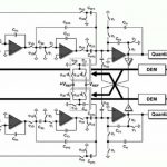
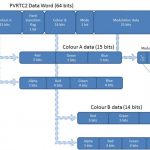
PVRTC2 is supported on the newest Series5XT or Series6 GPU cores from Imagination, retaining the modulated dual-image scheme found in PVRTC. The number of options for handling modulation data has effectively been doubled by using two new flags: an opacity flag for the entire data word, and a hard transition flag used for sub-texturing. The hard transition flag contributes to “non-interpolated” and “local palette” modes, which improve handling of discontinuities and contrasting colors.

Also introduced in PVRTC2 is support for NPOT (non power of two) textures, a feature defined in OpenGL ES 2.0. Prior to NPOT support, texture sizes had to be squared off up to the next power of two resolution, potentially wasting memory in many situations. In an extreme example, a 1600×1200 texture would have to be represented in a 2048×2048 surface. With NPOT, any size can be supported in PVRTC2; this is a big hitter removing one of the stronger objections to PVRTC.

So, let’s get to the question: how good is PVRTC2 decompression compared to other popular schemes?

PVRTC targeted block-level contemporaries and their primary shortcomings. Even the Ericsson team readily admits that ETC1 has weaknesses: “… if a block contains a number of pixels with very different chrominance, the results will be poor.” That may be overly self-deprecating, but captures the sentiment that efficiency is only part of the equation.

We see proof of “efficiency”, in terms of execution time, in a blog directly comparing the speed of ETC1 to PVRTC. The results show a big difference in initial load time (file size and memory bandwidth), and a significant difference in subsequent loads (how well the GPU and algorithm decompress the loaded images), especially applying 2bpp compression. But this poster concludes, as many others have, increased PVRTC 2bpp efficiency often comes at a price – in some situations, reduced visual quality. (I wouldn’t expect PVRTC2 to be a lot different in terms of execution time compared to PVRTC, but being supported on newer, faster GPUs may be a consideration.)

The other comment in that blog has to do with how PVRTC handles alpha transparency compared to ETC. Imagination obviously heard this type of feedback in designing PVRTC2, adding modes to handle alpha better. Game effects obviously rely heavily on transparency, but I’m intrigued by the recent debate on “flat” images in user interface design. iOS7 got a lot of criticism for going flat, but there may be some method to the madness: flat textures process a lot faster, and that can be a big contributor to a smoother user experience.

Let’s get back to overall visual quality. Eyeball tests with pixilated, jagged images yield fairly obvious conclusions when results degrade to the unacceptable. For the Imagination viewpoint, they offer a brief a case study on PVRTC2 discussing visual quality, but they only show comparisons with ETC and BC3 (one of the S3TC family) formats.

In the four test images Imagination selected – a synthetic image with color transitions, a photo, an icon typical of a user interface, and a game surface texture – it was a bit surprising to see BC3 look so bad. In this set, it is harder to tell the difference visually (at least on my monitor, and to get this to size up I had to JPG it at 100% quality which probably took out some differences) but PVRTC2 4bpp looks very comparable to ETC1 4bpp, and statistically it appears slightly better in some cases.

Many sources try to use a standardized set of compression test images like the Kodak lossless true color image suite, or the Tecnick Testimages set. For instance, Squish has done some outstanding work on the Tecnick Testimages set, comparing the statistical performance of most of the texture compression schemes available in OpenGL ES. Statistics are interesting, and one can debate the significance of some of these results. Most human eyeballs calibrate to a 2dB SNR difference, but we’d have to look much closer at standard deviation figures to see if pixelation and jaggedness are represented accurately.

For the moment, let’s take the Squish results at face value, assuming statistical figures of merit bear out in qualitative viewing. We notice PVRTC2 4bpp places right around ETC2 in most cases, only outstripped by some modes of ASTC. Interesting, ASTC was left out of the Imagination comparison … for several reasons; one is the caveat of “existing silicon” at the time of writing. ARM has the distinct benefit of late entry into this fray, with official release of ASTC in 2012, years after PVRTC debuted in late 2003. There is a great presentation on ASTC from its creators, exploring the issues they set out to address in engineering a newer solution.

Like some modes of an algorithm are better than others, there are also differences in technique that can affect results substantially. Obviously, the vast majority of images in a game or user interface are non-standard. I spent hours looking at image size and speed comparisons until finding this on improving PVRTC texture quality using Photoshop, which tells me (not surprisingly) just tossing images into the compressor and wondering why they come out fuzzy may not be the compressor’s problem. Some attention needs to be paid as to how images are designed prior to compression to get the best results.

courtesy Heyworks Unity Studio

Takeaways from this PVRTC discussion:
If you are selecting IP for an SoC, PVRTC2 is a solid choice running on a Series5XT or Series6 GPU. PVRTC is widely fielded, and state of the art is always advancing. Consider the end-to-end ramifications of software tools, GPU performance, compatibility, licensing, and other criteria when making a choice.

If you are writing apps for an Apple platform, you are already soaking in PVRTC2 – learn how to get the most from it. NPOT is a huge enhancement. 4bpp is solid, 2bpp should be evaluated carefully but it may be suitable for some images. The rebirth of flat design may be more than just an aesthetic trend, with tangible benefits in user interface performance.

If you are writing apps for Android, OpenGL ES embraces multiple texture compression formats which may or may not be supported in a particular mobile GPU – remember, software decompression in mobile is a bad, bad thing. To run in hardware on a variety of SoCs, most Android apps will need to deliver all OpenGL ES texture compression formats, perhaps using something like Adobe ATF as a container.

We’ve tried to give you a fair look at PVRTC in this series, showing what it does well and where there is room for debate. What are your thoughts and experiences?

More articles by Don Dingee…

lang: en_US


The Alternative to FinFET: FD-SOI

The Alternative to FinFET: FD-SOI
by Paul McLellan on 10-30-2013 at 11:00 am

Everywhere you turn these days you find FinFETs. Intel has had them since 22nm (they use the word Tri-gate but it is the same as what the world calls FinFET) and TSMC will have them at 16nm. So why FinFET? And is there an alternative?

The reason that regular bulk planar transistors have run out of steam is that the channel area underneath the gate is too deep and too much of the channel is too far away from the gate to be well-controlled. This is why leakage power (static power) has been going up so much: the gate is never truly turned off. Transistors are bright and dim not on and off. The solution to this problem is to make the channel thinner so that it is well controlled by the gate.

One way to do this is the FinFET. Instead of having a planar transistor with the channel in the silicon wafer itself, the channel is created as a thin vertical fin (like a shark’s fin, which is where the name comes from). The gate is then wrapped around three sides of the fin. Since the fin is thin, there is no part of it that is far from the gate and so the whole channel is well controlled by the gate. Leakage power goes way down. Life is good.


But is there another way to make the gate thin? Yes, it turns out that there is. Instead of making the channel area out of the silicon wafer itself, start with an insulator and add a thin layer on top of it to form the channel. Then build a planar gate on top of it in the normal way, along with source and drain. With the insulating layer at the back, the channel is thin and so, like in the FinFET case, it is well-controlled by the gate. Leakage power goes way down. Life is good.

This is the approach that ST Microelectronics is using with the not-exactly-catchy name of FD-SOI which stands for Fully-Depeleted Silicon-On-Insulator. The main coordination for FD-SOI technology is the SOI Industry Consortium. In addition to ST, semiconductor members include Freescale, IBM, GlobalFoundries, Samsung and UMC, although the detailed process roadmaps are not clear yet. Notable by their absence are Intel and TSMC who are both committed to FinFET exclusively.


FD-SOI has some advantages over FinFET since it is much more similar to a regular bulk CMOS transistor. The manufacturing is more of an incremental development from what has gone before and is simpler. So it should be cheaper to manufacture than FinFET (although the base wafers are more expensive). Design re-use is also much simpler.FD-SOI has a lot less variability due to the lack of implant, and in turn this means that the supply voltage for memories can be lowered by 150mV resulting in 30-40% power savings.

More information on FD-SOI is available on ST Microelectonics’ website here.


ARC EM SEP Processor, Safety Ready Solution for Automotive

ARC EM SEP Processor, Safety Ready Solution for Automotive
by Eric Esteve on 10-30-2013 at 5:24 am

If you are familiar with Processor IP core, you certainly know DesignWare ARC EM4 core, 32-bit CPU that SoC designers can optimize for a wide range of uses, and differentiate by using patented configuration technology to tailor each ARC core instance to meet specific performance, power and area requirements. If you develop a product addressing safety critical market, like Automotive or Medical, integrating a CPU core, you will need this processor to comply with ISO26262 standard. This means that the tool chain used to develop the processor has been audited and certified, the related safety documentation is available from Synopsys, and can be reused by the chip maker, and that the product itself is safety ready.

Let’s have a look at ARC EM SEP (Safety Enhancement Package) Core architecture, on the left side of the picture. If you compare it with ARC EM4 Core, on the right, you can immediately identify the safety related features: the blocks in green on the left, like Watchdog Timer, Lock-step interface or ICCM and DCCM where ECC/parity has been integrated.

The Automotive market is moving faster than ever to integrate more electronic content, this is true for entertainment, when a passenger can feel like being in a plane, watching a movie during a long travel, and this is also true for certain safety critical function like ABS or Body Control. The trend in Automotive Electronic is to localize processing close to the sensors to perform specific function, rather than using a central CPU, performing all these functions (just take a look at the picture below). Thus, you need a small footprint but powerful IP processor like ARC EM SEP, offering performance up to 300 MHz and power consumption as low as 16 µW/MHz on typical 65-nanometer (nm) low power silicon processes. And you need a processor core with integrated hardware safety features, so you can comply with ISO26262, and address safety critical applications.

To summarize, ARC EM SEP allow building distributed intelligence applications, thanks to automotive specific features set:

  • Optimized for high-efficiency, low-power embedded automotive applications
  • Automotive Safety Integrity Level D (ASIL D)-ready DesignWare ARC MetaWare Compiler streamlines development of ISO 26262-compliant software
  • Integrated safety features include parity support and error-correcting code (ECC) technology
  • Detailed IP safety documentation eases certification of ARC EM SEP-based systems

Like with other cores from ARC family, Synopsys customers can differentiate by creating own instruction, and gain market share on such a competitive market. Safety critical features integrated into ARC EM SEP should allow targeting Medical applications, expected to strongly grow in the future.

More Articles by Eric Esteve …..

From Eric Esteve from IPnest

lang: en_US


Social Media at Mentor Graphics

Social Media at Mentor Graphics
by Daniel Payne on 10-29-2013 at 5:52 pm

You can often tell how important blogging and social media is to an EDA company by how much effort it takes to find their blog from the Home page. For the folks at Mentor Graphics I’d say that blogging is quite important, because it shows up as a top-level menu item. Notice also how important Twitter is, their latest tweets show up on the Home page just below the logo, a prime real estate position for the web.
Continue reading “Social Media at Mentor Graphics”