llmda newsletter ad (2)

The hottest real estate? Your wrist!

The hottest real estate? Your wrist!
by Beth Martin on 12-19-2013 at 3:28 pm

I first read about the Pebble smartwatch earlier this year and thought “I don’t need yet another electronic device, and certainly not one that’s attached to my body.” Then I felt bad. Am I a troglodyte? It’s true, I do still have an iPhone 4, which is a little embarrassing in Silicon Valley. I have also never worn a wrist watch of any kind, but given the onslaught of smartwatches, I wonder how long I’ll be able to hold out. The options are growing, with companies big and small joining the battle for wrist-dominance.

The top selling point for a smartwatch in my opinion, is that it lets you keep your phone in your purse or pocket. The watch will alert you to incoming calls, emails, texts, tweets, Facebook posts, etc. Of course, this is also the main drawback. Another drawback is that none of these companies are able to design a product for women. Some out of this population of “most humans on earth” will don these clunky things anyway, but will still wonder why the smartwatch makers hate them. However, even if I never warm up to the idea, I’m convinced my husband needs one because he seems to miss many of my calls and texts, ahem.

But apparently many of the rest of the population is expected to buy a smartwatch. All the market forecasts indicate this business will go up and to the right; iGR predicts a CAGR of about 195% over the next five years into a $9 billion market. There are dozens in development, and they are also tapping into the growing health/activity monitor market. Most are Bluetooth accessories for your phone; some are standalone wrist computers. The sector is so hot that Qualcomm even has a horse in the race. CEO Paul Jacobs says he doesn’t really want to be in the gadget business, they are just trying to “drive the category forward.”

So, how to choose? I can’t pick based on looks alone (see comments above), I need to know what’s under the hood. Here’s some of my research on smartwatches available now or within the next few months:

[TABLE] border=”1″
|-
| style=”width: 91px” | SmartWatch
| style=”width: 164px” | Guts
| style=”width: 160px” | Other
| style=”width: 144px” | Notes
|-
| style=”width: 91px” | Pebble
| style=”width: 164px” | 120MHz STM32F205RG microcontroller, based on ARM Cortex-M3, Micron 32MB serial flash. 4 GB storage
| style=”width: 160px” | Lithium ion 130 mAh battery lasts 7 days. ST 3-axis accelerometer. Panasonic RF module with TI Bluetooth controller. Bluetooth 4 low energy. 144 x 168 pixel b&w Sharp memory LCD.
| style=”width: 144px” | Set a record for crowd source funding on Kickstarter, gathering over $10 million in their 37 day funding period. Works with IOS and Android. Available for $250.
|-
| style=”width: 91px” | Martian
| style=”width: 164px” | 400MHz CPU, 128MB RAM, 4GB storage, and It has 2 hr talk time, so instead of having to suffer people shouting into their Bluetooth ear-tumors, we’ll have to suffer people shouting at their wrists
| style=”width: 160px” | Lithium polymer battery lasts 2 hrs in talk mode, 7 days standby. Bluetooth 4 low energy. 3-axis accelerometer, glass crystal face. 96 x 16 OLED display.
| style=”width: 144px” | Analog quartz watch and a small alert window. Full voice commands, call, text, camera control. IOS and Android, but can’t use Google Now or Google voice. Available for $300.
|-
| style=”width: 91px” | i’m Watch
| style=”width: 164px” | ARM926J iMX233 at 454 MHz, 128MB RAM, Micron 4GB storage
| style=”width: 160px” | Lithium polymer 450mAh battery gives 5 hrs. 240 x 240 color TFT display. Focal Tech Systems FT5206 touch screen controller. ST Bluetooth, Wi-Fi, ST 3-axis accelerometer and compass.
| style=”width: 144px” | Italian-made smartwatch with full standalone cellular telephony, although the quality has been reported as poor. Make and receive calls. Android, IOS, Blackberry. Available now for $300, will increase to $400.
|-
| style=”width: 91px” | Sony SmartWatch 2
| style=”width: 164px” | 120MHz STM32F205RG, CPU, ARM Cortex-M3 based
| style=”width: 160px” | NFC and Bluetooth 3. 220 x 176 pixel display. 110mAh battery gives 2-3 days.
| style=”width: 144px” | Android. Available for $130.
|-
| style=”width: 91px” | Samsung Galaxy Gear
| style=”width: 164px” | 800MHz Exynos processor, 4GB storage, 512MB of RAM
| style=”width: 160px” | Super AMOLED display at 320 x 320 pixels. Wireless charging. 315mAh battery lasts one day.
| style=”width: 144px” | Currently works with the Galaxy Note 3. Call and talk capability. Apparently it’s not going over well; it has had a 30% return rate in the U.S. Available for $300.
|-
| style=”width: 91px” | Qualcomm Toq
| style=”width: 164px” | 200MHz low power ARM Cortex-M3 CPU
| style=”width: 160px” | Qalcomm’s Mirasol color e-ink screen, Qualcomm Bluetooth 4 controller. Wireless charging. 220mAh battery lasts 3 days.
| style=”width: 144px” | Supports Android. Available anytime now for about $300. Bonus: could be a collector’s item. Your grandchildren will be impressed or something.
|-
| style=”width: 91px” | Geak Watch
| style=”width: 164px” | 1GHz MIPS-based Ingenic JZ4774 SoC, 512MB RAM, 4GB storage
| style=”width: 160px” | 500mAh battery, Wi-Fi, Bluetooth 4, and NFC radios. GPS, sensors for temp, heartrate, blood pressure, and pulse.
| style=”width: 144px” | From Chinese company Geak. Available in US in 2014 for around $300.
|-
| style=”width: 91px” |
| style=”width: 164px” |
| style=”width: 160px” |
| style=”width: 144px” |
|-
| style=”width: 91px” | Neptune Pine
| style=”width: 164px” | 1.2GHz Qualcomm Sanpdragon, 16GB or 32GB storage
| style=”width: 160px” | GSM, 3G HSPA+, WCDMA, Bluetooth, Wi-Fi, micro-SIM, GPS, 5MP camera, 2.4 inch QVGA screen
| style=”width: 144px” | Standalone device running on Android 4.1.2. Pre-order for $335.
|-

The list of available watches is growing as I write this (and I’ve not even mentioned the hordes of ‘fitness’ devices that overlap in many functions with smartwatches.) There the MetaWatch, Casio’s G-Shock, Citizen’s EcoDrive, the Motorola MOTOACTV (now owned by Google), the Cookoo, Emopulse Smile, Kreyos Meteor, Kokkia, SVP G13 (award for catchiest name), and the Omate TrueSmart. Seriously, I can’t keep up so I’ll just stop now.

Apple, Google, and Microsoft are also working on their smartwatches. Apple’s smartphone is late, but has copyrightred the term iWatch, patented a “slap bracelet,” and hired a designer of the Nike FuelBand, so hopefully their product will be fancier than the current nerd-approved solution of taping an iPod nano to your wrist. Google bought WIMM Labs, who made an Android smartwatch in 2011 that had Bluetooth and Wi-Fi, 256 MB of RAM and a 667 MHz processor. It will be integrated with Google Now, is supposedly a few months from launch. Microsoft is reported to be in prototype testing phase of its smartwatch. Does anyone remember the Smart Personal Object Technology that Microsoft floated in 2002? Me neither, but I did find this picture. I guess they were ahead of their time.

More articles by Beth Martin…

lang: en_US


The Most Popular Blog Posts at Cadence in 2013

The Most Popular Blog Posts at Cadence in 2013
by Daniel Payne on 12-19-2013 at 11:42 am

I spend about an hour a day reading blogs from EDA companies, foundries, independent bloggers and of course, SemiWiki. Richard Goering at Cadence assembled a top 10 list of the most popular blogs posted on their site in 2013, revealing that engineers were most interested in: FinFETs, 20nm and smaller nodes, memory technology and PCB design.


Richard Goering, Cadence
Continue reading “The Most Popular Blog Posts at Cadence in 2013”


TSMC: 3D, 450mm, CoWoS and More

TSMC: 3D, 450mm, CoWoS and More
by Paul McLellan on 12-18-2013 at 4:29 pm

The first keynote at the Burlingame 3D conference was by Doug Yu of TSMC. Not surprisingly he was talking about 3D. In particular, TSMC has WLSI technology that they call CoWoS, which stands for chip-on-wafer-on-substrate which pretty much describes how it is built. This is the technology that Xilinx uses for its recently announced high end arrays which I already wrote about here.

The basic driver, in Doug’s view, is that on-chip interconnect is not scaling with Moore’s Law and so alternative approaches are required. He didn’t talk about cost (the manufacturers rarely do but when they talk about higher performance and lower power and don’t mention cost then you have to know the news is not wonderful. At best 20nm is flat to 28nm cost wise).

Another issue is that at 16nm FinFET it is not clear that everything we used to be able to integrate onto a chip, such as RF and analog, will still work. At least at acceptable cost. One obvious advantage of any sort of 3D chip is the ability to mix die from different processes, such as having a 28nm didital chip with 90nm RF/analog (what Doug calls “a ranch in the middle of Manhattan”) and move the 10um inductor off-chip. This saves chip area, cost and power.

TSMC is looking at how to ramp this 3D technology fast to volume. The costs of CoWoS are still too high but there is not really any substitute for the type of yield learning that comes from building products at volume. TSMC sees their goal to grow from a chip foundry to a subsystem foundry, delivering integrated subsystems consisting of die from multiple processes integrated together using CoWoS. He thinks that there are at most 5 companies that could potentially be suppliers into this market.

During questions he was asked about TSMC’s views on TSV holes. There are a number of ways of building TSVs. Via first means that the TSVs are created before the first layer of metal (I don’t think it is possible to do them before the transistors due to the high temperatures used in the FEOL, but I am certainly not a process expert). Via middle means that some metal is created and then the TSV is added and additional metal layers later to hook everything up. It is also possible to create the via from the backside of the wafer. The TSMC view is to do the TSVs as early as possible. Someone pointed out that you cannot use copper for the TSV if you do via first but Doug said that was not true and TSMC uses it today.

Eventually TSMC will scale all this to 450mm but it is too hard to move to 450mm at the same time as a node-change, so that 450mm will first be introduced on a node that is already running at volume. 28nm is my guess. But for wafer scale integration like CoWoS then 450mm is ideal since the costs are lower and they are not trying to get critical features to yield right out at the edge of the wafer where everything is more difficult.

The general impression from the keynotes at 3D ASIP was that:

  • 3D (which really means 2.5D and memory stacks for now) is real and 2014 will start to ramp
  • costs will come down with yield learning once a few million units have been built and shipped
  • driver will be high end initially (HPC, networking) not mobile, but mobile is the dream to really drive volume
  • the biggest problem is, surprisingly, not the TSVs but bond of the wafer onto a substrate for thinning, and then debonding the thin wafer afterwards and all the handling
  • interposers will have more than wires on. Once costs come down it makes no sense to leave the I/Os on a 20nm die instead of putting them on the interposers (they don’t really shrink anyway). Also power transistors, capacitors etc. If only wires, organic substrates will probably win.
  • component cost of a 3D chip will not be less than multiple components but the saving at the system level might be very large

More articles by Paul McLellan…


Complete IP port-folio built in less than two years!

Complete IP port-folio built in less than two years!
by Eric Esteve on 12-18-2013 at 10:47 am

We have posted several blogs related to Cadence IP strategy, or I should say new strategy. Each of these blogs was dealing with a particular product, like PCI Express gen-3 Controller IP, latest DDR4 Memory Controller or Wide I/O. This approach was equivalent to describe trees, one after one, and finally ignoring the forest! It’s possible to define a date, the T0 when Cadence has decided to consider implementing this new strategy to develop IP business: at the end of Q1 2012, when martin Lund came on board as Senior VP, IP Group. Since then, in about 20 months, Cadence has made numerous acquisitions: Cosmic Circuits, Evatronix, the SerDes Design Team of PMC Sierra and Tensilica, the latest being the most expansive and also the most ambitious. Engaging in the DSP/CPU IP core business is certainly a strong signal to the market that Cadence takes IP seriously! As far as I am concerned, I think that Cadence positioning in the Interface IP market is also a strong signal, and could be even more rewarding in term of volume of business on the mid-term, or within three to five years.

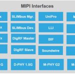
I was trying to better understand Cadence strategy for MIPI IP, as since Cosmic Circuit acquisition bringing MIPI PHY to the company at the beginning of 2013, MIPI IP port-folio has been drastically enlarged as you can see on the above picture. On top of the main and well-known interfaces like DSI, CSI-2, CSI-3, DigRF or LLI, Cadence has also developed UniPro, SLIMBus (Manager and Device), Battery Interface (BIF) and Soundwire. This sounds like a strong investment and illustrate a clear positioning: potential customer can find any of the MIPI interface he may need. If we look at emerging Interfaces like Mobile Express (M-PCIe), SuperSpeed IC (SSIC) or Universal Flash Storage (UFS), Cadence didn’t give it a miss and I guess that the R&D team should be busy developing these numerous IP.

Addressing the customer concern to consider Silicon proven IP solution rather than slides (extremely relevant care-about!), Cadence has integrated several of these MIPI IP into demonstration board, including M-PHY and D-PHY Test Chip. This is a good way to position MIPI IP as a potential winning solution: wide offer, Silicon proven PHY and Controller is clearly attractive.

As I have mentioned a complete IP port-folio, the above picture is the right illustration of Cadence ambition to propose as many IP solutions as possible, addressing various and different market segments: Mobile, Storage, Networking, PC and Peripherals and Consumer Electronics. Why investing so much? Because most of these IP represent a large and fast growing market! IPNEST has built the forecast for Interface IP (column 1, 3, 4, 5 and 6) up to 2017, the market associated will grow with a 12% CAGR during the next five years, reaching ¾ $Billion by 2017, see picture below:

Just a word from Martin Lund, from the still up to date September newsletter: “Cadence combined our expertise in interface IP, analog/mixed signal technologies, and system verification to offer customers a complete and full-featured NVM Express interface subsystem,” said Martin Lund, senior vice president, Research and Development, SoC Realization Group, Cadence. “Without this subsystem approach, SoC designers would need to source their interface component IP separately and drive integration on their own, often increasing their design risk and overall development time for new SoCs.”

Eric Esteve from IPNEST

More Articles by Eric Esteve …..

lang: en_US


Fab-U-Less! The 2013 Global Semiconductor Awards!

Fab-U-Less! The 2013 Global Semiconductor Awards!
by Daniel Nenni on 12-17-2013 at 9:00 pm

It was a dinner with more than a thousand semiconductor professionals from around the world keynoted by Author and Editor in Chief of Forbes Magazine Steve Forbes. What more could a humble blogger ask for? Even at $250 a plate it was well worth it just to mingle amongst the people who make this industry so great.

Global Semiconductor Alliance
Awards Celebration

It was a lot like one of the Hollywood awards shows with lights, music, videos, and of course speeches. Ballots were cast, winners were announced, trophies were handed out, acceptance speeches were made, applause applause applause… It was simply fabulous!

Most Respected Emerging Public Semiconductor Company Achieving $100 million to $250 million in annual sales Award and the winner is: InvenSense

Most Respected Public Semiconductor Company achieving $251 million to $1 billion in annual sales Award” awarded to Silicon Labs and the winner is: Silicon Labs

Most Respected Public Semiconductor Company achieving greater than $1 billion in annual sales Award and the winner is: QUALCOMM

Most Respected Private Company Award and the winner is: Aquantia

Best Financially Managed Company achieving up to $500 Million in annual sales Award and the winner is: InvenSense

Best Financially Managed Semiconductor Company achieving greater than $500 million in annual sales Awardand the winner is: Semtech Corporation

Start-Up to Watch Award and the winner is: Quantenna

Outstanding Asia-Pacific Semiconductor Company Award and the winner is:MediaTek Inc.

Outstanding EMEA Semiconductor Company Award and the winner is: NXP Semiconductors

Favorite Analyst Semiconductor Company Award and the winner is: MaxLinear

The most prestigious award, the Dr. Morris Chang Exemplary Leadership Award, was presented to CEO and Chairman, Dr. Sehat Sutardja and President and Co-founder, Ms. Weili Dai of Marvell Technology Group Ltd. (Marvell). A great “history of” video was included in this presentation. One thing I can tell you about Marvell is that they are very hard working people. Whenever I drive by their headquarters the parking lots are always full no matter what time of the day or night.

The only complaint I have, and I always have one, is that Steve Forbes did not mention Bit Coin or virtual currency in his economic policy keynote. Other than that, I agree with Steve that no matter how hard we work, no matter how hard we innovate, no matter how much fab space we build, unless people around the world prosper we, as an industry, will not. If you really want to know why the semiconductor industry has been relatively flat the last 5+ years look at the monetary policies around the world and the U.S. National Debt. It is a train wreck just waiting to happen, absolutely.

More Articles by Daniel Nenni…..


DAC 2014: Designer Track/IP Call for Submissions

DAC 2014: Designer Track/IP Call for Submissions
by Daniel Nenni on 12-17-2013 at 8:00 pm

Yes, it is that time of year again, DAC is coming and it is in San Francisco so you can bet we will break attendance records, absolutely. I would like to call on ALL semiconductor IP companies to exhibit this year. IP is the center of the semiconductor design universe, DAC is the premier semiconductor design event, and San Francisco is right next door to Silicon Valley, home of the largest semiconductor IP consumers, simple as that.

Semiconductor IP is today, and has always been, the highest source of organic (search based) traffic for Semiwiki.com: IP Integration, IP Verification, IP Qualification, and just about anything else IP.

MONDAY AT DAC: IP TECHNICAL TRACK

  • Keynote – Monday, June 3
    Sir Hossein Yassaie, CEO of Imagination Technologies

  • Invited Panel Sessions
    Providers & users on topics such as IP Selection, Verification & Export

  • Paper and Poster Sessions
    Users on their experiences building and deploying IP in the SoC’s, IP Verification & Software

IP EXHIBITS SoC PASSPORT PROGRAM

The DAC SoC Passport program assists attendees in finding the IP providers on the show floor, while providing an exciting platform to learn, network and win prizes.

  • DAC SoC Passport program is open to all exhibitors that provides IP or IP tools.
    All participating IP providers are listed on SoC Passport

  • Attendees can pick up an SoC Passport at:
    Main registration, IP company’s booth, DAC Pavilion

  • Attendees visit the IP providers during DAC; learn about the company’s IP offering; get a stamp in one or more categories listed on card
  • SoC cards must be turned in before the end of the show at the DAC Pavilion or DAC Registration to be scanned
    Complete cards will get a DAC IP t-shirt and entered to win the grand prize.

Program Benefits:

  • Participating in the program is free of charge to all exhibiting IP providers
  • DAC will promote program prior and during the show for full exposure and attendee awareness
  • Each participating company will:

    • Be listed on the SoC card with booth number
    • Be listed on t-shirt giveaway
    • Receive a stamp and SoC cards for distribution

SoC Passport Sponsorship:

  • Sponsors of the program will receive:

    • Logo on SoC card and t-shirt
    • Sponsorship recognition in promotional materials
    • Logo listed as a program sponsor on the IP SoC Passport website
    • Receive leads from turned in SoC cards

The DAC IP Track brings together Intellectual Property Core designers, users, and IP ecosystem providers. IP Designers and users from leading companies like ARM, Synopsys, Imagination, Intel, IBM, Samsung, TI, Toshiba, Qualcomm, and others will present their products and design experiences on effective design flows, methods, and tool usage.

IP Track Submission Categories:

  • IP Provider CPU / GPU
  • IP Provider Memory Controller / NOC
  • IP Provider Communications IP
  • IP Provider Analog / PHY
  • IP Provider Embedded Software
  • IP Management / Assembly
  • IP Verification

Submission details

Designer Track brings together IC designers and embedded software developers from across the globe. Designers and software developers from Intel, IBM, Samsung, TI, Toshiba, Qualcomm, AMD, Freescale, and other leading IC companies will present their design experiences on effective design flows, methods, and tool usage:

DT Submission Categories:

  • Front End Silicon Design
  • Back End Silicon Design
  • Embedded Systems & Software

Submission details

The Design Automation Conference (DAC) is recognized as the premier event for the design of electronic circuits and systems, electronic design automation (EDA) and embedded systems and software (ESS).

Members are from a diverse worldwide community of more than 1,000 organizations that attend each year, represented by system designers and architects, logic and circuit designers, validation engineers, CAD managers, senior managers and executives, and researchers and academicians from leading universities.

More Articles by Daniel Nenni…..

lang: en_US


Happy Holidays from Atrenta

Happy Holidays from Atrenta
by Paul McLellan on 12-17-2013 at 7:51 pm

It is that time of year and once again Atrenta has produced a video wishing you all the best for the holiday season. They are so spread around the world it is not just Hanukkah and Christmas but the Asian Lunar New Year (end of January) and probably some more holidays I don’t even know about. Last year there was a competition to name all the languages spoken in the video, but this year the countries are spelled out.

1 minute 10 seconds.

And Happy Holidays from me too!


More articles by Paul McLellan…


Security Path Verification

Security Path Verification
by Paul McLellan on 12-16-2013 at 5:18 pm

Formal approaches and security are a perfect match since you really want to prove that there are no holes in your security, rather than just being fairly confident. At the recent Jasper User Group meeting, Victor Purri presented some case studies in security verification.

The Jasper Security Path Verification (SPV) App is used to prove properties about the paths to secured data. For example,

  • Data in secure area must not be visible by CPU if it is not in secure mode
  • Secure register must not be written by non-secure agent

Usually data propagation requirements can usually be translated into one of these questions:

  • Can data on secure location A propagate to non-secure location B?
  • Can data on non-secure location X propagate to secure location Y?

In both cases we want the answer to be no, but it can be very hard to perform good verification without proper tools. Structural analysis can be very ad-hoc. Simulation depends on how good the verification engineer is at breaking the security. And standard formal verification is not a good fit since it is hard to describe the requirements as SVA/PSL assertions.

The SPV App is used specifically to address this need. The user specifies paths where data propatation should not occur and then the SPV App will act as a hacker and try and illegally overwrite secure data, or illegally leak secure data. This approach is exhaustive, efficient and correct.

The tool uses Jasper’s path sensitization technology. The tool inserts a unique tag, the taint, at the source and checks if it can appear in the destination’s signal. If so, then there is a path and a security violation.

One example Victor presented was that of a secure microcontroller which contains an encryption key. We want to make sure that it is not possible for the key to be leaked from the microcontroller. SPV proves that only the “key match” signal can be influenced by the key (and so it cannot be leaked that way). But that is not good enough, since we also need to check that the key match signal is correctly implemented. JasperGold inserts malicious instructions and finds a problem. A big one.

Note that the problem is not that our RTL is wrongly implemented, it is a hole in our overall security architecture. We need to extend the microprocessor architecture with an additional bit to tag instructions to indicate whether instructions are secure or non-secure.

SPV App is still an evolving methodology. The new tool ha a graph viewer and reachability analysis. In the future there will be support for bigger designs, different access interfaces and different security features.

There is more in the presentation. If you are a Jasper user (not necessarily one who attended JUG) then you can download the presentations, including this one, here.


More articles by Paul McLellan…


Why integrating HDMI 2.0?

Why integrating HDMI 2.0?
by Eric Esteve on 12-16-2013 at 8:47 am

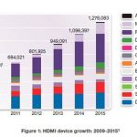
High Definition Multimedia Interface (HDMI) is today part of our day to day life, at home as well as at our office we are using devices integrating HDMI ports. HDMI penetration is well illustrated by this picture (created in Dec. 2011 by In-Stat): from DTV to Game console, the devices belong to the Consumer Electronics market segments, and we are supposed to use it at home. But we extensively use Mobile phones and PC (and peripherals) at work, as well as camera and camcorder for marketing purpose. According with this forecast, almost one Billion HDMI devices will have been shipped this year!

If HDMI protocol is such a success, why the “HDMI Forum” has decided to specify HDMI 2.0? The main objective was to support an ultra-HD experience with 4096 x 2160 pixels, the “4K” resolution, allowing viewers to watch video on ever larger screen with high definition clarity. But some HDMI 2.0 features are pretty attracting too:

  • HDMI 1.4 provided 10.2 Gbps aggregate (3 lanes at 3.4 Gbps) bandwidth, to support 4K x 2K Mode at 60 Hz and 24 bit color, you need: 18 Gbps aggregate bandwidth
Bandwidth = Horizontal pixels x Vertical pixels x (Frames/second) x (Color bits/pixel) x 10/8 TMDS encoding

  • Transition-Minimized Data Scrambling (TMDS) is implemented (above 10.2 Gbps only, to support backward compatibility with HDMI 1.3 and 1.4) to reduce EMI
  • New colorimetry format like YCbCr 4:2:0 offer a visual loss-less ultra-HD experience: don’t be confused by this “barbarian” name, such a format has been defined to provide a visual as close as possible to the human perception of colors!
  • New 21:9 frame format for true cinema experience
  • High-bandwidth Digital content Protection (HDCP) 2.2 for digital rights managements

If you want to know the full list of HDMI 2.0 features, I suggest you to read this excellent white paper from Synopsys: “How HDMI 2.0 Will Enrich the Multimedia Experience”.

It’s not really surprising to see that Synopsys is strongly involved in the new HDMI protocol version 2.0. IPNEST is monitoring the Interface IP market, including HDMI, since 2009. In the early days (2007-2010), Silicon Image was defining the standard, selling HDMI ASSP and also HDMI IP, collecting the royalties (through HDMI Licensing LLC.) and eventually running compliance testing of the protocol. Synopsys decided to penetrate HDMI IP market in 2010, and the company has developed PHY and Controller IP solution for HDMI 1.3, then 1.4 and now 2.0.

Because HDMI is considered as an additional feature to a large SoC, selling an integrated (PHY + Controller) solution was the winning strategy: a chip maker will not really differentiate by designing one or the other piece in-house. If you take a look at Synopsys web site, you will see that HDMI 2.0 IP includes the PHY, the Controller and even the Software. We don’t know the IP license revenues generated by HDMI for 2013, but I would not be surprised if Synopsys take the leadership –ranked before Silicon Image- in this segment. In fact, Synopsys has multiplied by 3 the HDMI IP license revenue between 2010 and 2012.

In the past, the semiconductor and electronics industry had some concerns with HDMI protocol: they had to pay royalties to HDMI LLC, but they could not influence the specifications. Until late 2011, HDMI LLC was a closed standard body that consisted in seven founders and over 1,000 adopters. The HDMI specification was architecture by the seven founders in a closed-door environment. In October 2011, the HDMI founders established a nonprofit corporation called HDMI Forum, with the purpose to foster broad industry participation in the development of future versions of the HDMI specification. The wide market penetration of HDMI protocol, covering every segment in Consumer Electronic, the consumer part of PC and Peripheral, the Mobile phone and even starting in Automotive segment, has made HDMI the de-facto standard for display technologies, and HDMI 2.0 the right solution for Ultra High-Definition Multimedia Experience.

From Eric Esteve from IPnest

More Articles by Eric Esteve …..

lang: en_US


Should Intel Offer Foundry Services?

Should Intel Offer Foundry Services?
by Daniel Nenni on 12-15-2013 at 11:00 am

This has been a heated topic since Intel announced that it would open its manufacturing facilities to the fabless ecosystem more than a year ago. I for one think it is a colossal mistake and I’m not surprised that many others share this view. IDM’s offering of excess manufacturing capacity to semiconductor design companies started the fabless revolution so this is Deja vu all over again. Those same IDMs are now fabless, fab lite, or out of business. Right?

Intel’s first foundry customers made complete sense. Achronix and Tabula are emerging FPGA companies meaning Intel can closely control the flow of process information. Achronix was an equity investment using the ASIC model where Intel does all of the heavy lifting so the process recipe never leaves the building. Ditto for Netronome. Altera however is more the traditional foundry model and this is where Intel crossed the insanity line, absolutely.

In order for Altera to compete with the likes of Xilinx they will need full access to Intel’s process technology and the ability to co-develop a process tuned for FPGAs. Altera and TSMC did this for many years up until Xilinx joined TSMC at the 28nm node. As a result, there is going to be a big shake-up in the FPGA market share numbers at 28nm. Historically Altera and Xilinx have been close but my guess is at 28nm Xilinx will run away with 70% market share which is exactly why Altera moved to Intel (they really had no choice).

From what I am told, the first versions of the Intel 14nm design rule manual delivered to Altera were redacted like something from the FBI. That has changed over time and the fact of the matter is that Intel’s process recipes are now available in the mainstream fabless semiconductor ecosystem which might as well be public domain. There are no secrets in Silicon Valley, especially now with semiconductor social media websites like SemiWiki.com, believe it.

For example: I know what the yield problem really was at Intel 14nm. It was not double patterning as many had guessed and technically it was a defect density problem as Intel had suggested but there was much more to it than that. Simply stated, it was increased CMP slurry at wafer’s edge causing excessive curvature which significantly limited yield.

Okay, back to the foundry question. Intel will not make money from Altera for many years to come and will be lucky to break even considering what a demanding customer Altera is. Same goes for Tabula and Achronix so this whole “filling the fabs” thing is a crock. Intel is just biding time until they can land a big SoC foundry fish which I don’t see happening. I work with SoC companies and they are not going to Intel, believe it.

Qualcomm Chairman Dr. Paul Jacobs said as much at a recent analyst conference:

Qualcomm Inc. (QCOM) BMO Technology, Media & Entertainment Conference December 11, 2013

The transcript is a good read if you are into the SoC business but here is the Intel as a foundry parts:

The other part of the question was about Intel what do we see about Intel as a potential source for foundry and I mean we’re certainly open to it, it’s — there they have expressed interest in going that way obviously TSMC and the other fabless guys have a different model right now for how they build their fabs they’re very flexible. They can run multiple different products through them simultaneously and it’s all software controlled where the cartridge of wafer go and Intel is famous we have been known for having a copy exact model, so they need very large volumes of a particular chip to run through that.

But I mean people change and so forth, so I mean it’s certainly interesting I mean I am glad to hear that their interested in going that way and we’ll see how that plays out. But right now I mean the fundamental of that in the foundry is that typically these leading edge chips go into a set of iconic phones an iconic phone is like a — it’s almost like a movie launch. Things happen in the first small period of time, so you have to ramp incredibly fast, build a lot of capacity on the frontend which means that after that those first wave has passed through that now there is a lot of foundry capacity leftover.

And the fabless model have to be there in order for other people to absorb that coming later, the later waves to absorb that. So I think the fabless model is very well suited to the mobile space and to these kind of leading edge designs and so I think it’s sort of necessary as a way of participating in the market.

Spin it any way you want but based on my experience with QCOM and the other top fabless companies there is no way they will be able to work within the rigid process requirements and the strict business demands of Intel. The foundry business just does’nt work that way. Unless of course they are desperate like Altera.

My advice: If Intel wants to fill their fabs, instead of giving $1B of chips away for free (Baytrail) and whoring out their excess capacity, Intel should acquire fabless companies that are in emerging markets to better diversify and do what Intel does best, make chips!

The Intel foundry guys sat at the table next to me at the GSA Awards last week which recognized the leading fabless companies around the world. Hopefully they made a shopping list of companies to acquire that can fill their fabs and return Intel to financial growth on par with the rest of the semiconductor industry (30% versus Intel’s 0%).