RVN! 26 Banner revised (800 x 100 px) (600 x 100 px)

Do You Really Know RapidIO?

Do You Really Know RapidIO?
by Eric Esteve on 05-06-2014 at 4:53 am

About 10 years ago, I was in charge of the product definition of our next IP to be released, the PCI Express gen-1 Controller. I was also involved in the decision process to select the new functions to develop, in respect with the market size, all of this being the definition of “marketing”. The reason why our company decided not to develop Serial RapidIO was because the engineering team was far too busy (PCIe IP sales were exploding). At that time, we also had Hyper Transport protocol in the radar. Fortunately, we did not select Hyper Transport, but we may have decided to add Serial RapidIO to our port-folio. Serial RapidIO is very complementary with PCI Express, as the protocol’s strengths are the PCIe’s weaknesses:

  • Serial RapidIO offers a very low latency (compared with PCIe, and Ethernet)
  • Serial RapidIO is a “routable” protocol: it can be used to interconnect a (very) large number of processors together (when PCI Express native topology is based on a tree: one Root agent is interconnected to several Endpoints)

If you want to dig more, and better understand the differences between PCI Express, RapidIO and Ethernet, you will find an excellent article, on RapidIO web site, in Technology Comparison section. The article is written by Sam Fuller, and Sam was a founder of the RapidIO Trade Association and now serves as Head of System Solutions, Digital Networking at Freescale Semiconductor.

Serial RapidIO protocol is successfully deployed in various applications, like DSP and Processor farms, Wireless 3G, WiMax and 4G base stations, Video servers, IPTV, HDTV or Media gateways, but also in Storage and Servers systems, Avionics and Space. We may expect a move from x86 to ARM based multicore processors in Storage/Servers, and such a move would be an opportunity to further deploy RapidIO protocol. It’s not a scoop that x86 and PCIe are often associated together (they are brothers, both Intel’s son!). Such an association is not optimal in Storage/Servers, especially when the goal is to interconnect a large number of devices, due to the native topology of PCI Express protocol (the famous Tree). We have seen some tentative to add to the PCIe specification some complexes addendum, namely Advance Switching (AS) or Multiple Rout I/O Virtualization (MRIOV), as matter of fact, these specification have not been widely adopted. A tree stays a tree, even if you try to multiply the roots, the PCIe native topology is not optimal, especially when you have to implement a very large Switch to interconnect the many processor that are present in a Storage or a Server architecture. Thus, we may expect to see wider adoption for RapidIO protocol, along with the emergence of ARM core based server/storage chip devices.

But we all know that even the most wonderful technology or protocol would be of no use without a large ecosystem, made of IP and VIP, Test Equipment, off-the-shelf (OTS) devices like Switch Fabric… and so on. On the PHY IP side, Serial RapidIO protocol is based on XAUI or Ethernet (10G ) signaling, any PHY IP vendor supporting these protocols will be able to support Serial RapidIO.

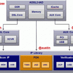
If you look at the above layered architecture, you can see that Mobiveil provides the Controller supporting SRIO 2.2, running up to 6.25 Gbps, as well as a controller extension, the RapidIO to AMBA AXI Bridge, allowing easy integration into any AMBA AXI interconnected SoC, in particular ARM CPU based processors.
You will find more complete information in Mobiveil product brief grio-pb.pdf

As I have written in one of the very blog in Semiwiki, “Design IP would be nothing without VIP”, and RapidIO Trade Organization has addressed this crucial need, as we can see here and below, extracted from the RapidIO web site:

RapidIO Bus Functional Model
The 10xN RapidIO BFM developed on behalf of the RapidIO Trade Association by Mobiveil supports RapidIO specifications 10xN (Gen3 version 3.0), 6xN (Gen2 versions 2.2 & 2.1) and 3xN (Gen1 version 1.3). The RapidIO BFM is developed in System Verilog and supports standard Universal Verification Methodology (UVM) and can be easily plugged in to any other UVM compliant verification components to extend a broader verification environment.

RapidIO BFM Features

  • 1x, 2x, 4x 8x and 16x lane configurations.1.25 Gbaud, 2.5 Gbaud, 3.125 Gbaud, 5 Gbaud, 6.25 and 10.3125 Gbaud lane rates
  • 66, 50 and 34-bit addressing on the RapidIO interface
  • All types of packet formats
  • Supports all types of IDLE sequences, Control and Status Symbols
  • Scrambling/De-Scrambling and Encoding/Decoding
  • Supports out of order transaction generation and handling
  • Critical Request flow (CRF)
  • Supports all transaction flows, with all priorities
  • Test pattern generation at all protocol layers
  • Error injection and error detection at all levels of protocol layers
  • Provides Compliance Test Suite
  • Functional Coverage

RapidIO was initially designed to serve as a processor fabric interconnect, and the protocol has most-often been used in embedded systems that require high reliability, low latency (typically sub microsecond) and deterministic operation. Using SRIO, low latency, high reliability and routable protocol should greatly help the expected explosion of ARM core based processor addressing the server/storage new applications. OTS devices, especially Switches IC from IDT, TI or LSI Logic are available, as well as RapidIO IP and VIP to support this new storage/server trend. PCI Express has been used in the past to support server/storage application, but we think that one of the main reasons was opportunistic: Intel, the market leader in these application, was obviously using x86 architecture, as well as (Intel strong promoter) PCI Express to support chip to chip interconnects, even if RapidIO would have given a better service in term of reliability and low latency. Moreover, RapidIO was defined from the beginning to serve as a processor fabric interconnects… but it was more strategic for Intel to use PCI Express than RapidIO (initially introduced by Motorola). Maybe it’s time for the server/storage industry to give a second chance to RapidIO protocol, which certainly deserve it!

From Eric Esteve from IPNEST

More Articles by Eric Esteve…..

lang: en_US


TSMC Updates: 20nm, 16nm, and 10nm!

TSMC Updates: 20nm, 16nm, and 10nm!
by Daniel Nenni on 05-05-2014 at 2:30 pm

*Spoiler Alert: The Sky is Not Falling*
The TSMC Technology Symposium last month provided a much needed technology refresh to counter aging industry experts (they make their living selling reports) who have been somewhat negative on the future of the fabless semiconductor ecosystem. If the sky wasn’t falling who would buy the reports, right? Let’s take a look at what Handel Jones of IBS reported last year and sync it up with what we learned from TSMC executives and symposium attendees last month.

Handel’s Chicken Little Conclusions:

[LIST=1]

  • 28nm will have a long lifetime with opportunities for equipment vendors to expand capacity inside China
  • 20nm parametric yield will improve and it will be a high volume technology node in 2015 but mostly 2016.
  • 16/14nm will provide low cost gates with volume production only in 2017.
  • 10nm will be postponed. Cost per gate will be prohibitive and unclear where demand will come from outside high-speed processors and FPGAs.

    First: Handel is RIGHT about 28nm having a long lifetime and it just got longer with the announcement by Jean-Marc Chery, COO of ST Microelectronics:

    “We have just signed a strategic agreement with a top-tier foundry for 28nm FD-SOI technology. This agreement expands the ecosystem, assures the industry of high-volume production of ST’s FD-SOI based IC solutions for faster, cooler, and simpler devices and strengthens the business and financial prospects of the Embedded Processing Solutions Segment.”

    Sources point to SMIC and the expanding low cost China mobile market which makes complete sense if you understand FD-SOI. Handel Jones has a white paper out titled “Why Migration to FD-SOI is a Better Approach Than Bulk CMOS and FinFETs at 20nm and 14/16nm for Price-Sensitive Markets. Paul McLellan wrote about it here. The discussion in the comment section is worth a read, absolutely. Maybe Handel will update that white paper to include 28nm?


    Second: Handel is WRONG about 20nm by one year. According to JK Wang, Vice President of Operations for 300mm fabs, TSMC will ship 300,000 20nm wafers in 2014 and 1,000,000 20nm wafers in 2015. The symposium attendees I spoke with confirmed 20nm is now in production with plenty of time for the holiday gift season.

    Third:Handel is WRONG again about FinFETs by another year. According to JK Wang, 900,000 16nm wafers will ship in 2015 and 1,300,000 wafers will ship 2016. Samsung supports this timeline saying 14nm will be in full production in 2015. And again attendees confirmed this.

    Fourth: Handle is WRONG about 10nm. According to Mark Lui, TSMC President and Co-Chief Executive Officer, 10nm will have multiple customer tapeouts in 2015 and risk production is planned for late 2016. 10nm is expected to provide a 25% performance increase, a 45% power reduction, and a 2.2X gate density increase over 14nm. 10nm will use existing immersion lithography equipment but will be “EUV compatible” if and when EUV is available. According to Paul McLellan, my goto lithography source, EUV is a big fat IF!

    Symposium attendees were a bit more skeptical on 10nm arriving on time but both Samsung and TSMC insist 10nm is well within the 2 year process ramp window. Given the great progress on Gen1 FinFETS I will play along with Gen2 roadmaps for now, absolutely.

    More Articles by Daniel Nenni…..


  • LSI’s Way of Faster & Reliable Electronic System Design

    LSI’s Way of Faster & Reliable Electronic System Design
    by Pawan Fangaria on 05-05-2014 at 9:30 am

    LSI Corporationstarted in 1980s and I had several encounters with it during my jobs in 1990s; not to forget the LSI chips I used to see in desktops and other electronic systems, and I’m happy to see LSI continuing today with more vigour having leadership position in storage and networking space. It provides highly reliable, high performance and power efficient network processors, communication chips and others for media, connectivity and storage applications. Last week, I was pleased to bump into an on-line webinarpresented jointly by Sudhir K. Sharma of Ansys Corp. and Dr. Cornelia Golovanov of LSI Corp. which made me learn how a system level design methodology used at LSI, involving Ansys Apache tools, leads them to precisely pin point the noise introducing elements in a large SoC including die, package and PCB with significantly fast multi-physics simulation technology and eliminate the same to improve reliability and performance of their chips.

    Sudhir talked about the advantages of miniaturization in semiconductor designs with multiple functions working together at low voltages and also introduced about the challenges to maintain their reliability amid high density and complexity leading to crosstalk, thermal and other electrical issues such as reduced noise margin with low operating voltage. It was interesting to note some of the natural phenomena such as mechanical fluid flow and signal attenuation caused by human touch needing a perfect harmony between electrical, thermal and mechanical systems that can handle any kind of variations within specified limits gracefully and predictably.

    Let’s look at an interesting case study about which Dr. Cornelia talked at length. This involves system level PDN (power delivery network) analysis including an IO ring sub-system where a bridging happens between power integrity of a PLL as influenced by the large current swings of a DDR PDN and the large signal swings of a DDR signal interface.

    The PG noise in the system can be due to switching activities as well as parallel resonances between PG planes and RLC series resonances and anti-resonances. The switching noise can be due to direct simultaneous switching of digital and analog cells generating transient current spikes and voltage drops. Also, an indirect cause could be due to PG acting as return path of current for switching signal nets; also capacitive coupling between digital and analog supplies. By using Sentinel-SSO, the full chip IO system can be analyzed and contribution of the IO ring switching established. The contribution of DDR signal activity to PLL power integrity can be analyzed and the noise at PLL metal1 pins due to coupling with DDR and chip, package and PCB can be monitored. The Sentinel-SSO enables the simulation of interaction between IO noise and PDN by using transistor models as well as macro models for the IO buffers.

    As shown above three different package bonding models were extracted upon soldering the package design onto the PCB. All data bit, address bit and control bit lines as well as the 1.8V and 1.8PLL supplies coupling were accounted.

    A 100ns simulation with transistor models takes 64 hours whereas the same withmacro models takes just 24 minutes producing similar results.

    Strong correlation of noise with the lab measurements was observed and LSI found the Sentinel-SSO based methodology to be highly instrumental in intercepting noise due to independently supplied IO cells switching activity severely impacting the dedicated VDDPLL and VSSPLL. Also, the system level workbench encompassing die, package and PCB interconnects exposed the impact of the capacitive and mutual coupling enabled outside the die on the PLL supply. A good correlation between results of pre-layout and post-layout flows was also observed. The methodology provided best selection of solution for PLL supply noise reduction.

    A GUI based workbench setup provided by Apache allows quick inclusion and exclusion of on-chip devices. The die can be viewed and analyzed at each layer and via to identify any design weakness. It allows scripting for fast setup of the workbench.

    Overall, I found this to be a very novel and robust approach for fast analysis and design of SoCs for high density and complex electronic systems which can meet the kind of PPA (Power, performance and Area) desired in today’s semiconductor community, yet be highly reliable in the long run. A detailed talk can be listened to by logging into the webinar here.

    More Articles by Pawan Fangaria…..

    lang: en_US


    Hardware/Software Debug

    Hardware/Software Debug
    by Paul McLellan on 05-04-2014 at 10:59 pm

    One of the big challenges with modern SoCs is that they have a complex software component as well as the hardware itself being complex. Some aspects of the hardware can be debugged independently of the software and vice versa, but often it is not immediately clear whether the source of a problem is hardware, software or some interaction of the two. A further complication is that typically the software engineers and the hardware designers are not the same people, often not even the same team (depending on whether the company is organized functionally or by project). But problems that span the hardware/software divide still need to be debugged.

    What is needed is a hybrid tool that consists of a software programmer’s view of the world, synchronized with a hardware view of the world. The programmer wants to see things like C-code, assembly code, variable values, register contents and so on. In a multi-core design then it gets even more complex since each core has its own set of values. At the same time the designer wants to see waveforms, RTL, assertions and all the other familiar features of Verdi debug. But both views need to be synchronized in time. If you single step a C instruction, the appropriate point on the waveforms needs to be indicated. Or if you see something suspicious in the waveforms, the appropriate code needs to be shown along with the other aspects of the processor state.

    Verdi[SUP]3[/SUP] from Synopsys is just such a tool. It shows simultaneous hardware and software views and enables a trace to be stepped forward and backwards to home in on problem areas with everything kept in lock step so you can seamlessly go between the two views of the design.


    Note that this is not a sort of virtual platform. The simulation is run and all the trace data is captured in FSDB as in a normal (hardware only) Verdi run. The Verdi hardware/software debug, which has gdb under the hood on the software side, can then be used to inspect what is going on. Without a tool like this, it is almost impossible to associate particular places in the waveform with the actual instructions being executed. In a mult-core environment, where several cores are often executing code simultaneously it is even more complex. See the picture above.

    The key features of the product are:

    • Complete software debug views including

      • Registers view
      • Call stack view
      • Variables view
      • Memory view
    • Fully synchronized hardware and software views: Jumping in any context in full simulation time range

      • Forward, backward
      • Statement in C, assembly source code
      • Waveform value changes
      • Selected simulation time
    • Supports breakpoint setting in C, assembly
    • Support simultaneous debug of multiple cores
    • Support several families of ARM cores as well as custom or proprietary cores

    The hardware and software views are shown below. Or they can be mixed with some aspects of software and some of the hardware all on the same screen.

    Alex Wakefield, a principal engineer at Synopsys, has a short video including a demo of Verdi hardware/software debug. It is about 7 minutes long.

    The video on Verdi hardware/software debug is here.


    More articles by Paul McLellan…


    The Number One ASIC Racing Team!

    The Number One ASIC Racing Team!
    by Daniel Nenni on 05-04-2014 at 9:45 am

    This weekend I was in the pits for the Flying Lizard Motorsports team at the Monterey Grand Prix. It was an auction item (donated by eSilicon) at EDA’s 50[SUP]th[/SUP] Anniversary party last year, and let me tell you it was an amazing experience and a very interesting story, absolutely. But first let me tell you that if you get a “Hot Lap” ride around a racetrack and the driver asks you how fast you want to go just tell him “no limit” and hold on for your life!

    The Flying Lizard team founder and lead driver is Seth Neiman. Seth was a vice-president at Sun Microsystems, a founder of Brocade Communications Systems, and served as a lead investor and board member of networking companies: Foundry Networks, Avanex, iPass, Shoreline, Juniper Networks and NexPrise. I’m guessing Seth wanted to be a race car driver when he was a kid? Seth was also lead investor of eSilicon, one of my favorite disruptive fabless semiconductor companies. eSilicon is a sponsor of Flying Lizards and that is how I met Seth.

    Jack Harding, the founding CEO of eSilicon, gave my beautiful wife and I the tour and primer on racing. Prior to eSilicon Jack was President and CEO of Cadence replacing Joe Costello. Jack came to Cadence from the $420M acquisition of Cooper and Chan Technology (CCT). Before he was CEO at CCT, Jack was Executive Vice President of Zycad which is where I first met him. Quite a few Zycad people followed Jack Harding to Cadence, unfortunately I was not one of them. Ever the contrarian, I went to Avant! which was later acquired by Synopsys after being sued into submission by Cadence. There was quite a bit of controversy behind the Cadence departures of both Joe and Jack but I will leave that to you folks in the comment section.

    You can read a brief history of eSilicon in the ASIC chapter of “Fabless: The transformation of the Semiconductor Industry” which is now available in print on Amazon.com. Much like what TSMC did for the fabless semiconductor industry, eSilicon transformed the ASIC business model into a success based relationship with customers. All current fabless ASIC companies now use this model where instead of paying design and manufacturing costs up front, customers purchase working chips. This success based business model has resulted in hundreds, if not thousands of design starts that we may have never had. Jack Harding and Seth Neiman are both semiconductor industry heroes, absolutely.

    After watching the Flying Lizards in action I can tell you that designing an ASIC today is not much different than winning an American LeMans race. Both require an absolute team effort. Members of the team each have their specific expertise and everyone depends on each person to be excellent at what they do. And if any one person on the team or any one tool fails an entire race can be lost. The difference is with an ASIC an entire company can be lost.

    About eSilicon
    eSilicon, the largest independent semiconductor design and manufacturing services provider, delivers custom ICs and custom IP to OEMs, independent device manufacturers (IDMs), fabless semiconductor companies (FSCs) and wafer foundries through a fast, flexible, lower-risk path to volume production. eSilicon serves a wide variety of markets including the communications, computer, consumer, industrial products and medical segments.

    More Articles by Daniel Nenni…..


    Leveraging Design Team Energy!

    Leveraging Design Team Energy!
    by Eric Esteve on 05-03-2014 at 5:12 am

    Once upon a time, in 1987 to be specific, a French design team was trying to develop a 100% Made in France supercomputer. In fact, not really 100%, as the CPU chips were supposed to be made by Weitek, but we never saw any of these chips, probably too challenging to be designed right first time! Anyway, I was in charge of the design of the functions which could be used by every other design teams – 4 or 5 ASIC had to be designed, using up to date design tools from VLSI Technology, as Synopsys Design Compiler was a bit too young at that time! Thus, I was in charge of:

    • Clock Distribution Arborescence (CDM did not exist, at that time) in the core
    • Clock distribution block for I/O reception
    • Clock distribution block for I/O emission (pretty complex function, asserted to the specific PVT of the emitting IC, eventually delayed to guarantee the Data Hold Time)
    • Master JTAG Cell
    • I/O JTAG Cell

    Nobody had ever proposed the concept of IP Reuse at that time, but every engineer involved in this supercomputer project was convinced that it was a good idea, so the design team in charge of the various ASIC designs could focus on the specific IC functionality. Twenty seven years later, the industry has put a name on this intuitively good idea and call it “IP Reuse”, moreover, a new tool family has emerged: IP Management tools, or Hardware Configuration Management, as described by Daniel Payne in this blog.

    Why using IP Management tool? The goals are multiple. The first goal is to guarantee the IP consistency across various design teams. We need to make sure that the Shanghai based team, designing the AUX Core interfacing with the ADSL2-IAD designed in San Jose, is using the same IP version than in San Jose. This is the same problem today that it was in 1987 in this supercomputer project: as soon as more than one design team is involved in the same project, you don’t want to duplicate design resource, and you want to make sure that exactly the same IP is used. Design productivity and IP consistency are the key words. This is the basic concept, but we think this concept should be extended. RTL IP has traditionally been defined as a design for which only RTL and simulation is available (soft IP), or a design, which has gone through synthesis and some placement information is available (firm IP) or has been taped out (Hard IP). But to improve design productivity it is important to broaden the scope of what has been traditionally defined as an IP. It can be extended to scripts developed to stitch the IO fabric together, regression scripts or verification test benches. Leveraging tested scripts and existing test benches help provide a jumpstart to design teams.

    This means that EDA vendors should go beyond simple IP Management tool, and extends the definition of the IP being managed by the tool into a more complex “object” made of:

    • RTL IP
    • + Verification Test Benches
    • + Regression scripts
    • + Placement information
    • + Routing information (when the same technology node is targeted).

    Since 1987, the chip maker company behavior has completely changed. Only very few companies decide to develop an ASIC once every two or three years, and in this case, they tend to pass through an ASIC company like eSilicon, OpenSilicon, etc. On the other hand, a large ecosystem of Fabless, Foundries and IP vendors has established. Then, we may think that a Fabless (or IDM) tend to develop as many ASIC as possible, around platform IC, to target many market segment… and amortize R&D cost. For these companies, better harness the energy of the designers, and reuse IP’s wherever possible, is just a way to improve economics.

    Adopting such a behavior will first require the right EDA tools, from ClioSoft for example, and also to push for mind change inside the company design community. At the IP source, the design team may have to provide extra effort to make the design reusable, at the IP sink, the well-known NIH syndrome will have to be thwarted. But this will be a low extra cost, compared with the benefit of harnessing the energy of the designers.

    From Eric Esteve from IPNEST

    Also Read

    Webinar: Making Design Reuse Work

    Importance of Data Management in SoC Verification

    The CAD Team – Unsung heroes in a successful tapeout


    Aldec is Celebrating 30 Years @ #51DAC!

    Aldec is Celebrating 30 Years @ #51DAC!
    by Daniel Nenni on 05-02-2014 at 8:00 am

    Dr. Stanley Hyduke founded Aldec in 1984 and their first product was delivered in 1985, named SUSIE (Standard Universal Simulator for Improved Engineering), a gate-level, DOS-based simulator. The SUSIE simulator was priced lower than other EDA vendor tools from the big three: Daisy, Mentor and Valid (aka DMV). Today, Aldec EDA tools are used to design, simulate and verify FPGA, ASIC, SoC and embedded system designs. There are over 35,000 users of Aldec tools with distribution in over 43 countries. Aldec remains one of the few privately-held EDA companies with a 30 year history, while in that same time period the EDA industry has seen literally hundreds of smaller companies get acquired by larger ones.

    Aldec will sponsor DAC’s annual Monday Night Networking Reception (SemiWiki will sponsor Tuesday’s reception). All registered DAC Attendees and Exhibitors are invited to join and celebrate Aldec’s 30 Year Anniversary with free cocktails, hors d’oeuvres, cupcakes and prizes. CUPCAKES!!!!

    DAC Monday Night
    Networking Reception

    Monday, June 2, 2014
    6:00pm – 7:00pm

    Moscone Center Esplanade Foyer

    Technical Sessions and Demonstrations
    June 2-4, 2014 from 9:00am-6:00pm at Booth #1521

    Session 01: Quick Intro to SCE-MI
    Session 02: OSVVM: Advanced Verification for VHDL with Synthworks
    Session 03: SoC Emulation Made Easy
    Session 04: Visual Mapping: GPS for UVM Journey
    Session 05: High Level Synthesis with NEC
    Session 06: Requirements-Based Verification
    Session 07: Design Rule Checks in FPGA design
    Session 08: Prototyping over 100M Gates
    Session 09: Ask Aldec: Demos, Roadmaps, Partners, Q&A, etc.

    1-on-1 Sessions fill up quickly. Visit http://www.aldec.com/dac2014to register. Choose one or more sessions and schedule a time that is convenient for you.

    About Aldec
    Aldec Inc., headquartered in Henderson, Nevada, is an industry leader in Electronic Design Verification and offers a patented technology suite including: RTL Design, RTL Simulators, Hardware-Assisted Verification, SoC and ASIC Prototyping, Design Rule Checking, IP Cores, Requirements Lifecycle Management, DO-254 Functional Verification and Military/Aerospace solutions. www.aldec.com

    lang: en_US


    FD-SOI : SMIC or…Who else?

    FD-SOI : SMIC or…Who else?
    by Eric Esteve on 05-01-2014 at 9:12 am

    In fact, as of today, nobody can refer to an official statement made by any STM executive about name of the foundry able to process FD-SOI wafers in 28nm. We just know that the agreement is about to (or has been) signed… But we may speculate, and try to use our rational thinking. For example, the Semiwiki readers had the opportunity to read this article, back in November 2013: “IP-SoC 2013 Top Class Presentations”. As I am living in France, going to Grenoble is much easy for me than for Paul or Dan, and I have presented to IP-SoC numerous times since 2007.

    In this article, I have expressed my questioning about SMIC presentation, as this was not really a Foundry sales pitch but rather a corporate message from China Inc. I have no issue with it, I was just surprised. I must say today that I better understand why the presentation from SMIC was organized this way, if we assume that SMIC executives came to Grenoble not only to present to a couple of hundreds European designers… but also to discuss business with their STMicroelectronics counterpart. Let me add that it was the first time ever that SMIC went to IP-SoC to present…

    This above slide shows you that I mean by “Corporate pitch from China Inc.” If you miss this article, just take a look at this paragraph:

    The presentation from SMIC was also interesting, for a different reason. Tian Shen Tang, Sr VP, SMIC, has delivered a sale pitch for SMIC, as expected, and this pitch was even more a China sales pitch. It was certainly a good idea to remind the audience that China is moving fast, very fast. If ten years ago western companies were searching for a low labor cost resource, Chinese OEM, semiconductor and Design IP companies are now competing with their western counterpart. It was a surprising presentation, but the message delivered by SMIC makes sense, and the company is positioning as a partner, helping Design IP to penetrate Chinese market. If you prefer, it was more a business oriented (political?) than a pure technical message, but the message was clear: China is part of the High Tech market, and SMIC can help you addressing this market.

    Another slide from IP-SoC 2013, presented by Giorgio Cesana from STM:

    I have recently posted a comment to a post from Paul (FinFET vs FD-SOI) and clearly identified the current weaknesses of the FD-SOI business proposal (and how these weaknesses could be removed):

    This lead to the last point. I really think that FD-SOI is a great technology, which can be use to fab chips at a lower cost, or at lower power-or higher performance- for the same cost. The magic is that you can gain one technology node, like stay in 28nm, but with the power or performance benefit of 20nm. But, in the real life, to attract customers, you need to open two doors:

    • Wafer double sourcing
    • Manufacturing double sourcing


    Each of these being a show stopper. Let’s assume that SOITEC and STMicroelectronics are working these business issues, then the next issue is to develop a large enough ecosystem around IP and EDA. This is more like a chicken and egg issue, but, as soon as the right amount of money will have been invested to make sure that the right IP are available, the design-win will generate enough cash will be invested to enlarge the ecosystem. This is not as magic as the technology, it’s just a question of business decision, strategy planning and business development!

    If we consider the (pseudo) scoop made 6 months ago in Semiwiki in this article “IP-SoC 2013 Top Class Presentations”, at least one gate has opened, and FD-SOI is on the way to be a credible technology, to be used to attack the very busy consumer and mobile segments!

    From Eric Esteve from IPNEST

    More Articles by Eric Esteve…..

    lang: en_US


    More “toddlers” innovating on the IoT

    More “toddlers” innovating on the IoT
    by Don Dingee on 05-01-2014 at 8:00 am

    As the PC Era took shape, Tom Peters predicted the shift away from “where all the cars are parked”. He foresaw that large, established companies would no longer be the economic engine, or the dominant force in innovation. Smaller firms, even individuals, would rise to prominence in a new, technologically-driven economy.

    That turned out to be a very solid call. With semiconductors, software, and systems from new players, more jobs and more ideas started coming from new companies. This shift has accelerated as the Internet, fabless, and open source technology have further leveled the playing field and removed many barriers to entry.

    In the Post-PC Era, we’ve seen the results. Smartphones and tablets exploded on the scene, pulling through more SoCs and IP and software and tools (including EDA), putting more technology firms on the list of household names. The maker movement and crowdfunding have enabled innovation on a scale never before seen, launching even more ideas.

    Perhaps the biggest idea so far is the Internet of Things. Ask 20 people at random what is the IoT, and you probably get 20 slightly different to substantially deviant answers. There are certainly some leading use cases – home automation, mHealth and quantified self, connected cars, beacons, smart grid, and the list goes on – that draw a lot of discussion.

    When there is no one answer, opportunity abounds. Now, we don’t even know exactly where the cars, all or just a few, are going to be parked. Gartner research analyst Jim Tully made a very prescient remark last year indicating just how wide open the IoT is for innovation:

    Our research says that by 2018, 50% of the Internet of Things solutions will be provided by startups which are less than 3 years old. We can estimate what the Internet of Things will be like now. But we know that most of the things that will exist in 2018 we can’t even conceive of because they haven’t been invented yet.

    We have most of the building blocks of IoT technology today – microcontrollers, operating systems, wireless sensor networks, MEMS sensors, cloud computing, and more, enabling devices to be created. In many cases however, the technology precedes the business model. It is essential to launch a new design cheaply, and likely iterate or even pivot the solution several times, before a sustainable revenue stream is tapped.


    Toddling toward an uncertain future with little money in hand but a wealth of creativilty, many startups opt for open source software, often never bothering to look at commercial code – and that is a shame. Skipping past commercial code “just because” based on financial or philosophical grounds can miss what could have been a winning combination best for both the developer and the end user. I always advise my clients that cost and religion should be the last two factors in a trade study, not the first two.

    Free speaks very loudly to most developers, however. What if IoT startups could gain access to proven commercial software technology, backed by decades of operating system, development tool, and microcontroller experience shipped in billions of units, for the low, low price of zero dollars to get started?

    Mentor Graphics and Atmel have just teamed to launch an Atmel-enabled version of the Nucleus Innovate Program (joining NXP, ST, and TI offerings), offering free licenses of the Nucleus RTOS and Sourcery CodeBench tools targeting Atmel SAM3x and SAM4x for qualified businesses under $1M in annual revenue. Mentor Embedded is taking a proven strategy – in-depth understanding of device architecture achieved by working closely with a semiconductor vendor, reflected in an optimized kernel, compiler, and debug tools ready for prime time – and extended it from SoCs into microcontrollers.

    If the trend Tully has identified holds course, and the projections of 50B or more devices are true, innovators will come from everywhere. The IoT and its startup toddler hopefuls will need a lot more tools – open source and commercial. This hybrid model, where a commercial software vendor incents startups with limited cash to design in and deploy production-ready code at no cost, may set a precedent for the next phase of innovation.

    lang: en_US


    Semiconductor Cost Models: Boring But Crucial

    Semiconductor Cost Models: Boring But Crucial
    by Paul McLellan on 05-01-2014 at 5:00 am

    One of the most important and underrated tasks in a semiconductor company is creating the cost model. This is needed in order to be able to price products, and is especially acute in an ASIC or foundry business where there is no sense of a market price because the customer and not the manufacturer owns the intellectual property and thus the profit due to differentiation.

    For a given design in a given volume the cost model will tell you how much it will cost to manufacture. Since a design can (usually) only be manufactured a whole wafer at a time, this is usually split into two, how many good die you can expect to get on a wafer, and what the cost per wafer is. The first part is fairly easy to calculate based on defect densities and die size and is not controversial. There is some guesswork involved ina a new process since you have to price volume production at the yield you expect to be able to achieve even though early in the life-cycle of the process you can’t.

    In fabs that run only very long runs of standard products there may be a standard wafer price. As long as the setup costs of the design are dwarfed by other costs since so many lots are run in a row, then this is a reasonable reflection of reality. Every wafer is simply assumed to cost the standard wafer price. In fabs that run ASIC or foundry work, many runs are relatively short. Not every product is running in enormous volume.

    Back when I was at VLSI we initially had a fairly simple cost model and it made it look like we were making money on all sorts of designs. Everyone knew, however, that although the cost model didn’t say it explicitly the company made lots of money if we ran high volumes of wafers of about 350 mils on a side, which seemed to be some sort of sweet spot. Then we hired a full-time expert on cost-models and upgraded the cost-model to be much more accurate. In particular it did a better job about the setup cost of all the equipment when switching from one design to the next, which happened a lot. VLSI brought a design into production on average roughly daily and would be running lots of designs, and some prototypes, on any given day. The valuable fab equipment spent a lot of the day depreciating while the steppers were switched from the reticles for one design to the next. Other equipment would have to be switched to match the appropriate process because VLSI wasn’t large enough to have a fab for each process generation so all processes were run in the same fab (for a time there were two so this wasn’t completely true). Intel and TSMC and other high volume manufacturers would typically build a fab for each process generation and rarely run any other process in that fab.

    The new cost model shocked everyone. Finally it showed that the sweet spot of the fab was high volume runs of 350 mils on a side. Large enough that the design was complex and difficult (which we were good at) but small enough not to get into the part of the yield curve where too many die were bad. But the most shocking thing was that it showed that all the lower volume runs, I think about 80% of VLSI’s business at the time, lost money.

    This changed the ASIC business completely since everyone realized that, in reality, there were only about 50 sockets a year in the world that were high enough volume to be worth competing for and the rest were a gamble, a gamble that they might be chips from an unknown startup that became the next Apple or the next Nintendo. VLSI could improve its profitability by losing most of its customers.

    Another wrinkle on any cost model is that in any given month the cost of the fab turns out to be different from what it should be. If you add up the cost of all the wafers for the month according the cost model, they don’t total to the actual cost of running the fab if you look at the big picture: depreciation, maintenance, power, water, chemicals and so on. The difference is called the fab variance. There seemed to be two ways of handling this. One, which Intel did at least back then in the early 1990s, was to scale everyone’s wafer price for the month so it matched the total price. So anyone running a business would have wafer prices that varied from one month to the next depending on just how well the fab was running. The other is simply to take the variance and treat it as company overhead and treat it the same way as other company overhead. In the software group of VLSI we used to be annoyed to have our expenses miss budget due to our share of the fab variance, since not only did we have no control over it (like everyone else) it didn’t have anything to do with our part of the business at all.


    More articles by Paul McLellan…