llmda newsletter ad (2)

SpyGlass CDC: A Comprehensive solution for addressing CDC issues

SpyGlass CDC: A Comprehensive solution for addressing CDC issues
by Pawan Fangaria on 06-19-2014 at 7:30 am

About a decade ago, semiconductor designs had just a few asynchronous clocks which were easily managed by designers through the process of manual design reviews. The situation today is completely different. An SoC can have hundreds of asynchronous clocks, driving different complex functions, spread across various IPs, supplied by different vendors. It’s just not possible to analyze the interaction of all these asynchronous clocks manually, and even the traditional tools are not sufficient. Tools need special intelligence to recognize the synchronized and unsynchronized crossings between various asynchronous clocks to identify design issues. In the SoC verification arena, Clock Domain Crossing verification is at the forefront of RTL verification because a single CDC issue, if not resolved well, can result in design failure forcing an expensive design re-spin.

Knowing that Atrenta’sSpyGlass® has a comprehensive solution for CDC analysis, I fixed up an appointment with Paras Mal Jain, Director Engineering at Atrenta, to learn about their SpyGlass CDC product. Paras has been involved in the development of the SpyGlass CDC product from the very beginning when customers started demanding an automated tool for handling CDC issues. It was an interesting conversation involving intricate details about CDC in general and the SpyGlass CDC product in particular.

Q: Paras, I hear these days, CDC has become a big issue in SoC Verification. I also hear that you have a comprehensive solution for this. Tell us more about the solution.

A: Yes, CDC has become one of the most dreaded problems in SoC designs. The issue appears when signals cross asynchronous clock boundaries without being synchronized. It’s difficult to catch CDC issues precisely by using traditional tools which may either under-report real design issues and / or over-report false violations; static timing analysis and RTL simulation tools are not suitable to identify the CDC problems. We have a state-of-the-art solution with a strong structural CDC verification sign-off flow, proven across a very large number of customers. We also offer solutions for SoC level CDC analysis and functional CDC verification. Then, there is also simulation based dynamic CDC verification for certifying the SoC design to be CDC safe, i.e., CDC sign-off.

Q: What kind of structural analysis is done? More importantly, how are the identified issues resolved?

A: SpyGlass CDC provides a rich suite of rule-sets to verify all kinds of structural CDC issues. To begin with, it helps in validating the user setup to ensure that CDC verification does not result in bogus violations. Next, it identifies unsynchronized and synchronized clock domain crossings. There can be numerous unsynchronized crossings detected, but the real value of the product is in performing the protocol independent analysis to enable identification and filtering out the false negatives upfront.

For Example:

· Paths that can be between clocks of two slaves that never interact among themselves
· Crossings due to quasi-static signals and crossings between other groups of signals that don’t require synchronization
· User defined synchronizers

SpyGlass CDC provides flexibility to the user to define custom synchronizers. By eliminating the majority of false violations, SpyGlass CDC saves lots of the designers’ time and allows them to focus on real design issues.

Other structural CDC checks include convergence and reset verification. Another important aspect of CDC verification is analysis across power domains without power logic instrumentation. This helps users identify the CDC issues which would otherwise be shown after power logic instrumentation. As part of its CDC methodology, SpyGlass CDC provides guidance to users throughout the design and validation process. It also helps users identify the inputs such as the synchronous and asynchronous reset signals. Additionally, it also identifies quasi-static signals that need to be ignored during investigation and analysis for unsynchronized crossings.

Q: What is protocol independent technology?

A: SpyGlass offers low noise CDC verification using protocol independent synchronization checks. With this technology, we identify generic synchronization elements as opposed to rigid structures. We don’t need to necessarily chase around RTL specific structures which may be design style dependent. Depending on rigid RTL structures can be error-prone and it is almost impossible to detect all RTL styles; protocol independent analysis is immune to design structures and can identify FIFO, handshake, and other synchronizers that are properly designed in a generic way. It identifies critical signals for a clock domain crossing which may synchronize the crossing structurally and it also checks if it would make the crossing work functionally correct.

Our protocol independent synchronization verification is a patented technology and can exhaustively verify any CDC problems in a holistic way and provides ease of debug. This is seamlessly integrated into the SpyGlass Platform.

Q: How are the functional checks done?

A: The functional checks are done to ascertain that the circuit is working properly without any data loss, data incoherency issues, or glitches in the design. The functional checks are necessary because structural CDC analysis only makes sure that synchronizers are in place to avoid metastability, but functionality of the synchronization circuit is verified using functional verification. Assertion based verification techniques are used to perform the functional checks. The assertions are inferred automatically without requiring any user intervention and then they are verified using advanced formal engines. For example, in case synchronized signals are converging in the design, they should be gray-encoded. SpyGlass CDC automatically infers such signals and verifies them automatically, to ensure they are gray encoded using formal verification techniques. Use of a wide range of formal engines, abstraction refinement techniques, multi-core features, and support of verification languages such as OVL / SVA results in a comprehensive and productive functional verification.

We have a combined methodology for both structural and functional verification to perform early CDC sign-off.

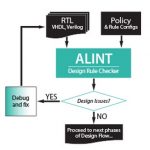
Q: This seems quite interesting. Considering the SpyGlass RTL sign-off solution, how is the overall flow constituted? How are the issues substantiated from RTL to Gate level, because there can be a few structural changes, if not more, between the two?

A: There are primarily three types of verification – structural, functional, and dynamic, as shown in the figure below:

At the RTL, substantial structural analysis and functional analysis is performed to find all CDC issues. At the gate level, insertion of clock gating, power optimization logic, or some other net-list level changes may introduce new CDC issues. Therefore, it is mandatory to perform complete structural analysis. The functional verification is done as required depending upon the fixes done during structural analysis.

Q: What is your experience from customers with the product?

A: Our customers have been extremely positive. Most of the top 20 semiconductor companies and over 150 customers are using the SpyGlass CDC solution. It’s the market leader in the industry for identifying CDC issues at the IP level, as well as the SoC level. We have many success stories from our customers who avoided re-spins of their chips by using SpyGlass CDC.

This was a very absorbing conversation with Paras, and I could gauge the finer handling of the issues by SpyGlass CDC that provides automated and comprehensive guidance to the users.

SpyGlass CDC provides comprehensive CDC signoff including structural and functional CDC analysis, ease of debug, low noise and highest performance for very large size designs.

Atrenta has organized a free live webinar on ‘Signoff Quality CDC Solution for Billion+ Gate Designs’. Here is the schedule –

Date: Wednesday, June 25, 2014
Time: 10 AM PDT

Interested people can register to reserve the slot and know more about CDC.

More Articles by Pawan Fangaria…..

lang: en_US


Embedded Vision Summit: the How-to and the How-to

Embedded Vision Summit: the How-to and the How-to
by John Swan on 06-19-2014 at 12:08 am

When I realized I had the opportunity to attend the Embedded Vision Summit (EVS) if I would change a return flight to a day earlier, I didn’t hesitate. Thankfully I was able to change my flight without any nuisance fee from the airline, and attended EVS.
There were two “How-to’s” at this Summit:

  • The algorithmic How-to, which includes

    • Object detection
    • Object recognition
  • The design How-to, which includes

    • IP aspect
    • EDA tooling aspect

The morning Keynote presentation, “Convolutional Networks: Unleashing the Potential of Machine Learning for Robust Perception Systems” by Yann LeCun, of Facebook and New York University, was a good example of the algorithmic How-to. Object detection is difficult enough, with objects moving in several ways: translationally (across the field of view), moving closer or farther, rotationally around an axis, and changing shape – like a person reaching out their arms, or even talking. Even more difficult is object recognition.

Not a lite keynote, LeCun dug into the algorithm and experimental results. The algorithm has a brief learning process after which it is able to give good probabilities that the object matches with one for which it has gone through the learning process. LeCun demonstrated the algorithm by using an attached webcam to his PC and aiming at different scenes from the podium: His face, his shoes, the right side of the audience, the left side, etc. After aiming the webcam and pushing the Learn button he was then able to aim the camera at the various scenes and showing a probability histogram of what learned ‘object’ the scene matched with. LeCun Presented for an hour and kept the audience captivated. Just when you thought he might be wrapping up he was pushing on to something new.

Jeff Bier has the design How-to expertise, which I have been aware of since about 1997 when I was at Motorola Corporate Labs. Jeff has always been up on DSP design tooling – it fits with the traditional them of BDTi which he founded to do DSP processor benchmarking. Multimedia such as embedded vision (if you can call it multimedia) is the next higher-order of signal processing.

Jeff did 2 presentations, one entitled “What’s New in Tools for Vision Application Design and Development?” In order to extract knowledge from embedded vision we rely on the hardware: processors, sensors, etc.and the Software: algorithms, libraries, APIs – the tools to get both of them together and working. Jeff highlighted 3 main software development environments: OpenCV, OpenCL, and OpenVX, an emerging Khronos standard API providing a vision hardware acceleration (abstraction) layer. Khronos has information on OpenCL and I will leave it up to the reader to do some further research on those. Jeff also told us about development kit for support of embedded vision.

After attending this Summit I intend to attend the future Summits!

You can access the Summit presentations here if you are registered on the Embedded Vision Alliance website.

(Submitted from DAC, where there’s a lot more on the How-to)

lang: en_US


What is Authentication and Why Should You Care?

What is Authentication and Why Should You Care?
by Bill Boldt on 06-18-2014 at 10:00 pm

Authentication means making sure that something is real, just like it sounds.In the real world, authentication has many uses. One of the most recognizable is anti-counterfeiting, which means validating the authenticity of a removable, replaceable, or consumable client. Examples include system accessories, electronic daughter cards and spare parts. Of course, authentication is also employed to validate software and firmware modules, along with memory storage elements.

Another important and growing role for authentication is protecting firmware or media by validating that code stored in flash memory at boot time is the real item – effectively helping to prevent the loading of unauthorized modifications. Authentication also encrypts downloaded program files that can only be loaded by an intended user, or uniquely encrypt code images that are accessible on a single, specific system. Simply put, authentication of firmware and software effectively makes control of code usage a reality, which is important for IP protection, brand equity maintenance and revenue enhancement.

Storing secure data, especially keys, for use by crypto accelerators in unsecured microprocessors is a fundamental method of providing real security in a system. Checking user passwords via authentication means validation – without allowing the expected value to become known, as the process maps memorable passwords to a random number and securely exchanges password values with remote systems. Authentication facilitates the easy and secure execution of these actions.

Examples of real-world benefits are quite numerous and include preserving revenue streams from consumables, protecting intellectual property (IP), keeping data secure and restricting unauthorized access.

But how does a manufacturer ensure that the authorization process is secure and protected from attack? With hardware key storage devices such as Atmel’s ATSHA204A, ATECC108A and ATAES132 – which are all designed to secure authentication by providing a hardware-based storage location with a range of proven physical defense mechanisms, as well as secure cryptographic algorithms and processes.

The bottom line? Hardware key storage beats software key storage every time – because the key to security is literally the cryptographic key. Locking these keys in protected hardware means no one can get to them. Put another way, a system is not secure if the key is not secure – and the best way to secure a key is in hardware. It is that simple.

Bill Boldt, Sr. Marketing Manager, Crypto Products Atmel Corporation


TSMC (TSM) is Having Another SoC Year!

TSMC (TSM) is Having Another SoC Year!
by Daniel Nenni on 06-18-2014 at 9:00 am

TSMC’s stock has more than doubled in the last five years. Coincidentally that is when I started blogging about TSMC. QCOM stock has experienced a similar doubling during this time as have other TSMC customers. The question is: What is next for TSMC? As I have mentioned before, you would be better off taking stock tips from your dog but this is what I see for this year and next for TSM.

Apple will become one of TSMC’s largest customers in 2014. This is simply amazing to me as I grew up with Apple as a computer hobbyist. Apple started selling mother boards before selling complete computer systems. In fact, I was at the UC Berkeley Campus when Steve Jobs entered wearing a backpack with a Macintosh computer inside ushering in a new era of personal computing. And now Apple is one of the largest fabless semiconductor companies? It boggles the mind!

The quarterly wafer ramping numbers I have read for Apple are $0 to $700M per quarter this year starting in Q2 2014 and up from there depending on the success of the iPhone6 and iPads to be announced later this year. As I have mentioned before, I predict that the iPhone6 will break revenue records and it is filled with TSMC silicon, absolutely. Given that TSMC will ship 300,000 20nm wafers in 2014, Apple will probably consume most of them. The other SoC vendors are still scrambling to get 64-bit 20nm SoCs taped-out. Apple really disrupted the SoC business with their 64-bit A7!

In 2015 Apple business could result in an additional $1B per quarter for TSM. Based on what I heard at #51DAC the TSMC/Apple relationship will continue into the FinFET era. One interesting note; I saw quite a few Apple badges at #51DAC, which was not the case at #50DAC. Those Apple engineers are becoming more plentiful and less stealthy it seems.

QCOM however is TSMC’s largest customer. QCOM consumed a record number of wafers last year, roughly a 50% YoY increase. FinFET is the big question, will they go TSMC or Samsung? I can tell you for a fact that QCOM will not use Intel Foundry, nor will any other SoC vendor that has a choice. It may have something to do with Intel flooding the market with free 22nm SoCs? Let’s see how many of those 40 million “contra revenue” parts actually make it into consumer’s hands. Ironically Intel will be using TSMC 28nm for their new Sofia SoC but I would not expect any volumes there either unless Intel goes contra revenue again.

The latest word from #51DAC is that QCOM will straddle TSMC and Samsung for FinFET wafers to get better margins. TSMC’s margins are at an all-time high (36%) and QCOM’s are at an all-time low (16%) so you do the math. A Samsung/QCOM foundry relationship seemed like a natural fit since Samsung is one of QCOM’s largest customers but with the launch of the Samsung Exynos SoC in 2010 the two companies are now frenemies. As they say, keep your friends close but your enemies closer. That is from the book “GodFather II” by the way. Michael Corleone said, “My father taught me many things here — he taught me in this room. He taught me — keep your friends close but your enemies closer.”

The other SoC vendor that I track is MediaTek. They are literally down the street from TSMC and UMC so I see them during my Taiwan travels. MediaTek is an interesting company that has done extremely well in the low end SoC business. I view MediaTek, TSMC, and UMC as brothers so I highly doubt they would use GlobalFoundries or Samsung but it is certainly possible. In this business margins are everything.


Aldec Can Ensure Smooth System Integration

Aldec Can Ensure Smooth System Integration
by Luke Miller on 06-17-2014 at 9:00 pm

Tools, tools, tools. Designs are rapidly changing, JESD204b, Hybrid Memory cube and all other Gigabit serialization schemes are here to stay. RIP DDR. This means board level simulations with respect to firmware (FPGA) are going to be more challenging than ever. Why? you ask, especially if the board layout is simpler? True, but the data pipes are faster and wider, FPGAs denser, causing the board to do more in the same space. What tools are you going to use? I hate process but it is necessary.

Aldec has a neat tool that should place everyone on the same page within a team. Cowboys beware, this is not for you and you may find yourself at another ranch, move over Hoss. The tool is called ALINT. It is a VHDL/Verilog design rule checker. I know, it does not sound glamorous but let’s face it, the steps to successful design if often not to glamorous.

So let’s walk thru a real example. Say you are the team leader or product team lead for the firmware part of a surveillance RADAR. You are responsible for the beamformer, pulse-compressor, doppler filter. The requirements are traced and you get 6 guys and/or gals for the firmware design of the FPGAs. Two people per function. Now, unguided your beamformer VHDL/Verilog will look very different from the doppler or pulse-compressor teams. For the FPGA clock, some may call it clk, Clock, clk_p. Reset may be called rstn, nrst, rst… Signal names may be a crap shoot. Some folks on the team may use state machines that have the ‘others’ clause, some may use every state. Some may use synchronous reset, some asynchronous, other’s using none assuming default to ‘0’ state. Now each design may simulate correctly and verified against a golden set of data generated by our good ole Octave (You thought I was going to say MATLAB… ok MATLAB too). So what is the issue? All the designs worked in simulation, and let each code their own style and way, why cramp their style? What kind of team leader do we have here? Quick call HR!

The problems, I can almost guarantee will arise during the best part of FPGA design, system integration. Having a common set of VHDL/Verilog design rules such as naming conventions, coding styles, state machine, reset, clocking, signal types… would go a long way on simplicity of debugging and finding errors that would not show up in RTL simulation but in integration such as that ‘Random’ word that is dropped every 14.6 seconds. The other benefit is anyone else can pick up the same code and understand it. How many times has that happened to you? You get the design thrown over the wall from another designer and yikes! You almost have to start from scratch.

There are many more benefits of ALINT such as custom rule creation, phase based linting (you cannot get to the next step until the simplest of warnings are fixed), DO-254/ED-80 support… Check out the tool over at Aldec, and give it a try. I truly wish I had a tool like this years ago!

lang: en_US


Five Things You Don’t Know About MunEDA

Five Things You Don’t Know About MunEDA
by Paul McLellan on 06-17-2014 at 3:00 pm

So first the one thing that you do know. MunEDA are based in Munich which makes them German. I have to confess that until I got involved helping them a bit with some marketing stuff that that was about all I knew about them too.

So now five things that you might not know:

1. MunEDA have a much wider customer list that you know and would even expect. Partially this is because most of their customers are outside the US, largely in Asia. But they are silicon proven by global customers in wireless, memory, automotive, communication, industry, IP and others. Their tools are used by 10 of the top 20 semiconductor companies. Altera is a noteworthy US customer.


2. MunEDA run annual user group meetings in both Europe and Asia with extensive presentations from leading edge customers. These are then archived for their customers as a reference. They have been doing this for years so now there are literally hundreds of presentations by users on how to use MunEDA’s tools effectively.

3. One of MunEDA’s areas of expertise is in variation analysis. This is a growing problem but took a step up in complexity at 20nm with double patterning. The two patterns are not self-aligned so depending on whether the gap between two lines is the minimum or the maximum can make a big different to the performance. Variability is only getting worse with each process node too. MunEDA have the only functional and silicon proven ultra high sigma yield analysis method for 6=9 sigma. To infinity and beyond. Ultra High sigma variation analysis is one of the primary uses that Altera is making use of MunEDA’s tools. Other areas that MunEDA excels in, low power consumption, optimizing circuits for performance enhancements and statistical circuit analysis.


4. One of the next big problems that you haven’t paid enough attention to? Aging and reliability analysis. The smartphone SoC market has made us all lazy since we throw our phones away faster than the chips age or fail. But automotive, aerospace, health and medical. They are all on their way. People get really upset if their cars don’t last fifteen years or more. And those chips are not in such a benign environment as your pocket or purse. They are under the hood where it is hot and vibrating a lot (or, if you go to Canada, cold). And medical? It really ruins your day if you have to have your chest opened to have your heart pacemaker replaced. MunEDA have aging an reliability analysis tools to address all this stuff and proven in silicon.

5. MunEDA is privately held and profitable. They just brought Pete Hansen on board to run their US operations and extend their success in the rest of the world to the US market too. Pete was my VP sales when I was CEO of Envis and then went on to get Solido into many flagship accounts.


More articles by Paul McLellan…


Xilinx KCU105 Evaluation board is key for your demo

Xilinx KCU105 Evaluation board is key for your demo
by Luke Miller on 06-16-2014 at 5:34 pm

I love God, my wife, kids, and FPGA boards. I know I am not alone, there are other nerds out there, don’t be shy. Friday my “Kintex® UltraScale™ FPGA KCU105 Evaluation Kit” came in. Think about this, this is real 20nm Xilinx FPGA hardware that really works. Below is a nice picture of all the swizzles the board has.

I believe this is the first 20nm FPGA board available. I know, this board is obviously lacking an rs-232 port. I hate going thru the USB. I’m old fashioned. My favorite interface is anything fiber. I love fiber, and could be the spokesperson for Metamucil. Anytime I use these boards, I usually use fiber protocols such as VITA17.1/.2 or Fiber Channel. Some of you may pop the card into your PC and use PCIe. Some may use Ethernet, others USB. The point is the KCU105 handles all your interface demands.

The FMC expansion site, FMC1 will quickly let you integrate advanced new standards such as JESD204B, or an x8 Hybrid memory cube. Need memory? DDR4 is on board, already pinned out, ready to be accessed. Flash memory is also available to meet the needs of you that need coefficients or stored data to remain when the power goes off. The heart of this board is the XCKU040 in a -2 Speed Grade. That -2 speed grade means you can run the DSP at 661 MHz, it has 1920 DSP for a potential 2.5 TMACS, not bad!

Me being a RADAR fella, I plan to start playing with some algorithms using MATLAB, coding some C, using Vivado HLS and seeing what I can do. Times have really changed for me in two major areas with FPGA design. Back in the early days, I would have to wait for a custom board to come back, get tested and verified, and then I could test out all my hand written VHDL on the board. I must say this process was not smooth and seemed to make management very cranky. Today I can have my design ready and a Xilinx board around the same time to get near instant gratification. With less errors using Vivado HLS and IP Integrator, as I am no longer hand coding nor using custom CCA’s. Those of you that must have custom needs, and that is many of you, say for some anti-tamper requirements can still use the KCU105 evaluation board. It will allow you to verify your design with all the interfaces you need. When the custom board comes in, you have 99% confidence that if things are no worky, then the issues are perhaps on the custom hardware side. But remember it’s never the software guys 😉

Another trend I am seeing is very aggressive demo/design schedules. It seems that the end customer is not so interested in documents and power point but working demo hardware. Having this board for your demo could be the difference of winning or losing a bid. Xilinx is well aware of this, as I have one of the KCU105 board sitting on my desk. The question is will you have one? Expect availability by the end of the year and shipping in Jan 2015.

lang: en_US


National Semiconductor Education in the Cloud

National Semiconductor Education in the Cloud
by Paul McLellan on 06-16-2014 at 1:28 am

“I wandered lonely as a cloud,” wrote Wordsworth. Well, clouds are pretty lonely in EDA these days. Despite some of the advantages on paper that mean that companies from salesforce.com to Netflix make heavy use of cloud-computing, semiconductor design has barely touched the cloud. One exception was Nimbic (acquired by Mentor last month).

There are many reasons, and there have been several discussions about this already on semiwiki. The biggest ones to my mind are:

  • security: big fabless (and IDM for that matter) companies have policies in place that their intellectual property does not leave the premises. Every time there are reports in the press that passwords have been stolen or other breaches, those policies only get stricter
  • all or nothing: the data volumes involved in designs are so large that either the whole design is done in the cloud or none of it is. It is not really feasible to move designs back and forth. Plus trying toe maintain a design environment in the cloud that is identical to the one locally hosted is a herculean task
  • commercial terms: to get everything into the cloud requires cooperation with the EDA companies on the terms of licenses, and this hasn’t been worked out yet. If you are going to have computing on demand you also need EDA licenses on demand.
  • status quo. the companies who might be expected to dip a toe in the water already have internal CAD groups, internal farms, EDA contracts and adding a few percent of additional cloud resource just adds problems

Instead, the place to start experimenting with the cloud is somewhere that doesn’t have any of these problems:

  • no massive IP issues so no massive security concerns
  • no existing infrastructure so can get going with a cloud-only approach
  • no commercial terms required
  • no status quo so can start from scratch

Sounds too good to be true. But it turns out there is somewhere just like that. Universities in countries that don’t really have very much in the way of IC design infrastructure. But universities don’t really have any money so you can’t just go to the universities and sell them a cloud solution.


However, “Nation building” countries such as Singapore, Malaysia, Saudi Arabia, Morocco, Egypt, Brazil, Vietnam, Pakistan have all targeted IC design as a way to move to a knowledge-based economy, move up the value chain and increase per-capita income. They all have government institutions charged with making things happen in this area. With budgets. Today, although these countries all wonder how to get an Intel or equivalent to set up a group there by tweaking tax policy, the reality is that without designers you can’t pay them to go there. Their big weakenss is that their countries don’t graduate enough designers, dozens rather than hundreds or thousands.

Silicon Cloud International has been targeting these institutions with the proposal to set up a complete cloud-based design environment. They will be the CAD organization for the entire academia of these countries. Instead of being paid by the universities (and in these countries they have even less money than in the US or Europe) they are paid by the institutions charged with getting things going. If they graduate lots of designers then there is scope for locally-based entrepreneurs doing things, or for established semiconductor companies to set up design groups there.


The SCI environment includes all the tools from all the usual suspects (who supply them for free). IP and PDKs are all there too. To address security issues they do something that sounds insane at first. You can neither upload nor download anything. As long as the designs are completely created in the SCI environment then there is no need for it. They already have an agreement with MOSIS so you can tape out without requiring to download anything.

To further address security and IP issues, the cloud based design environment can only be accessed through a Chrome-based thin client. After all, very little local computing power is needed, this is cloud-based. There is not even local storage. The clients cost around $200.


Universities in places like the US are also interested but for different reasons. They are perfectly capable of maintaining their own design environment but it doesn’t really add any value to the university for either teaching or research to do so, it is pure overhead.

What stage are they? The prototype has been active since September last year and a pilot program will start late July.

“All at once I saw a crowd,” Wordsworth continued, “a host of golden daffodils.” Well SCI are hoping to host their own crowd…but of students not daffodils.

More information on SCI’s website here.


More articles by Paul McLellan…


Product Marketing & the Butterfly Effect

Product Marketing & the Butterfly Effect
by Randy Smith on 06-15-2014 at 7:00 pm

I often feel that product marketing can simultaneously be an underrated and overrated function. More often than not, it suggests product goals, pricing, and positioning. Then the marketing department must defend those positions to both engineering and sales. However, both the engineering and sales departments can claim expertise for technology, purchasing patterns and customer desires. In my view, this is the difference between success and failure in the product marketing function – becoming a part of a successful well-integrated team. Product marketing should be a uniting force inside the company. Failure to bring in all voices and enabling enlightened decisions can have huge unexpected results.

When we founded Tangent Systems, I was an engineer. It was the extreme generosity of my co-founders that enabled me to also pursue an MBA at Santa Clara University while we were building Tangents initial products. I didn’t take a full course load, which enabled me to have the best chance to keep pace with my engineering and management responsibilities. When I did complete the MBA, I moved into product marketing, a natural transition for someone with a BSEE and an MBA. Eight months later, Tangent was acquired by Cadence, its very first acquisition. The deal closed in January 1989.

Tangent had two primary place and route products: TANCELL, a channel router-based tool that was the first timing-driven tool on the market; and TANGATE, one of the first commercial area routers. At the time of the acquisition of Tangent, Cadence already had two other channel routers, Symbad from ECAD, and Edge Place & Route by SDA. As Cadence had been formed only recently by the merger of these two companies, there were four product marketing directors – two each from SDA and ECAD. Rod Dudzinski and I, the two product marketing people from Tangent, were assigned to positions which kept us out of the process of deciding what to do with the collection of channel routing products. Bruce Bourbon, Cadence’s Executive VP of Marketing gave me the opportunity to work on product marketing of Design Framework II, as well as participate in all four strategic planning committees. It was not an unreasonable decision under the circumstances, and I have nothing but gratitude for the way that Bruce has mentored me over the years.

Ultimately the decision was made to go forward with Edge Place & Route as it was the only tool integrated in the Cadence Framework. This really amounted to an engineering view of the product. In fact, a deeper analysis of the customer base would have revealed that TANCELL customers were focused on ease-of-use and Edge Place & Route customers were the polar opposite, as they wanted detailed control and integration of the editor. These were two different markets, ASIC standard cell, and structured custom design. The insular approach to product marketing at that time missed this key market reality.

In 1991, Eric Cho, a marketing director not involved in place & route, left Cadence as one of the co-founders of ARCSYS. The first ARCSYS product was ArcCell which clearly targeted the former (and some diehard current) TANCELL customers. This opening made it possible for ARCSYS to gain traction. In time, Gerry Hsu would leave Cadence beginning what was termed “probably the most dramatic tale of white-collar crime in the history of Silicon Valley” by BusinessWeek. Avant! went public, based on a valuation significantly derived on stolen source code. The cash from the IPO allowed Avanti! execute a string of mergers. In 2002, Synopsys bought Avant! and settled the long running lawsuit with Cadence for $265M.

In the end, Synopsys had acquired so many successful product lines through its acquisition of Avant! that it briefly surpassed Cadence as the overall EDA revenue leader in fiscal 2003, and then moved to its current leadership position by 2008. Some of the dip in revenue by Cadence under the Fister regime might be attributable for this, but Cadence’s latest rise is a credit to Lip-Bu Tan’s leadership.

While Synopsys’ long steady increase in revenue is a bi-product of Aart DeGeus’ pragmatic mentality, there is little doubt that the Butterfly Effect of a small product marketing decision at Cadence in 1989 ultimately led to the Synopsys surge after the Avant! acquisition in 2002. Product Marketing decisions are critically important, even the seemingly little or obvious ones.

lang: en_US


FinFET Based Designs Made Easy & Reliable

FinFET Based Designs Made Easy & Reliable
by Pawan Fangaria on 06-15-2014 at 11:00 am

Although semiconductor manufacturing has taken off with FinFET based process technology which provides lucrative payoffs on performance improvement, power reduction and area saving in devices for high density and high performance SoC demand of modern era, apprehensions remain about its reliability due to reduced noise margin, EM and ESD tolerance, and increased heat generation. The increased level of switching due to high density of circuit at higher peak currents and higher grid impedances lead to higher voltage drops, and that combined with reduced supply voltages affects both noise margin and power significantly. The increased voltage drop heightens temperature and thus affects EM reliability of devices as well as interconnects. The FinFET technology also exhibits poor diode protection and that coupled with reduced interconnect reliability can render the chip vulnerable to ESD issues.

So, how to tackle these issues in order to avail the nonpareil advantages of FinFETs? I like Ansys’snew offerings in its RedHawk 2014 platform. My sincere appreciation for Ansys’s effort to proliferate the learning about the real challenges of FinFET technology and how to use RedHawk 2014 to estimate, measure and analyze various parameters to sign-off the semiconductor design at full-chip and package (including 3D stacks) level for power, noise and reliability with silicon correlated accuracy, pico-second resolution and maximum sign-off coverage.

After an overwhelming response to Ansys’s presentation on RedHawk 2014 capabilities to analyze and sign-off FinFET based designs in DAC, they are now unveiling a free webinarfor a larger audience across the world which will provide details about the challenges involved in FinFET based designs and amid those challenges how to address power, noise and reliability sign-off by using RedHawk 2014. The webinar will also provide information about RedHawk certification for 22nm, 16nm and 14nm FinFET processes from multiple foundries.

The new attractions are DMP (Distributed Machine Processing) providing major capacity and performance boost for billion transistor designs including multiple IPs, CPA (Chip-Package Co-Analysis) providing accurate power integrity and reliability analysis including the package impact on die, and temperature-aware EM methodology.

The above image provides a glimpse of package impact analysis on DvD (Dynamic Voltage Drop) with RedHawk-CPA; it considers distributed parasitic network with pin-to-pin mapping.

There are powerful connectivity checks which can determine grid and design weaknesses including power/ground balance, resistance issues, missing vias, static IR, high power density, placement of pads, switches and so on.

The robust reliability checks include power and signal electromigration, chip and system thermal modeling, ESD, clamp placement, cross domain, current density and so on.

The power & noise sign-off includes package-aware chip simulation and chip-aware package simulation with multi-domain power up/down analysis. The vector, vectorless and mixed-excitation analyses are done to improve sign-off coverage along with accuracy. Timing hotspots are also analyzed along with the DvD map.

To know details about these technologies and methodologies, it’s worthwhile attending the webinar. Here is the schedule –

Date: Wednesday, Jun 25[SUP]th[/SUP] 2014
Time: 11:00 AM PDT
Register here to reserve your valuable time and participation in the webinar.

I am excited to hear Calvin Chow, Area Technical Manager at Ansys-Apache, who will provide a great insight into FinFET technology challenges, various tools within the RedHawk 2014 platform and their capabilities to address the reliability of semiconductor designs with FinFETs within the realm of these challenges. Stay tuned to hear more on this.

More Articles by Pawan Fangaria…..

lang: en_US