llmda newsletter ad (2)

SemiWiki is an Open Forum for Semiconductor Professionals!

SemiWiki is an Open Forum for Semiconductor Professionals!
by Daniel Nenni on 06-15-2014 at 10:05 am

Why should you be a part of SemiWiki? Two reasons: One, SemiWiki is an excellent semiconductor networking tool. Quite often “who you know” comes into play in your professional life so network-network-network. Two, SemiWiki is all about personal branding. Establish yourself as a person of interest in your chosen field and opportunities will come to you, absolutely.

Today everything and everyone is connected and crowd sourced. In fact, all social media, from blogs, to forums, and wikis have a profound impact on how people communicate, search for information, and make decisions.

If you are a SemiWiki member you can blog, start forum discussions, create wikis, post events to the calendar, send private emails to other members, etc… As an example, the SemiWiki calendar is a high traffic area. When you post an upcoming event your picture and a link to your profile appears with it for all to see. Seriously, I get stopped quite frequently with a, “Hey you are one of the SemiWiki guys!”

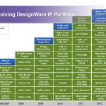
Another example is wikis. The most popular wiki contributed by a member has been viewed more than 37k times. This list is a compilation over many years of mergers and acquisitions in the EDA market. The original compilation was done by an individual (Ian Getreu) and is not an official list associated with any company or organization:

A Compilation of EDA Company Merger Listing All the Logos an EDA Company Owns

As a SemiWiki Member you may adopt a screen name to protect your identity but you must register with real names and your LinkedIn profile. Only semiconductor professionals with LinkedIn profiles qualify as SemiWiki Members and all Member information will be held in the strictest confidence. SemiWiki does NOT rent, sell, or trade member information.

Branding works best when you use your real name but that is your choice. I started blogging five years ago and have found it to be an incredible experience. It was rough going in the beginning. In fact I cringe when I look back at some of my first blogs. Fortunately, over the years we have developed a blogging recipe and we would be happy to share it with you. It is a bit of work but at the end of the day you will find writing to be a mind expanding experience, absolutely. And if writing a book is on your bucket list blogging is a great start!

While Google, Yahoo, Bing, and other search engines will continue to play an important role in social media, KNOWLEDGE SHARINGsites like SemiWiki are the new search. The role of user generated content has changed the way information is exchanged. SemiWiki brings technology and technologists closer together than ever before, providing in-demand content and facilitating peer-to-peer communications using Web 2.0 technologies.

User generated content through open collaboration is also called conversational media. In the case of SemiWiki it includes more than one million semiconductor professionals and people interested in the semiconductor industry collaborating around the world. SemiWiki also works closely with more than 40 companies in the fabless semiconductor ecosystem and that means access. Just imagine the possibilities…

More Articles by Daniel Nenni…..


Sensor Hub and Wearable Gestures

Sensor Hub and Wearable Gestures
by Paul McLellan on 06-13-2014 at 10:00 am

One of the challenges with the internet of things (IoT) is that many devices are both always on and battery powered (and not with a large battery). The responsibilities need to be split so that the device senses when it needs to wake up without requiring the application processor to be waking up all the time to make the decision since that would rapidly use up all the available battery power.

Quicklogic last week made two announcements, one a sensor hub for wearables and the other specific gesture algorithms especially for watch like devices worn on the wrist. Two gestures that are important are tapping on the device (like you do with a FitBit for example) or rotating your wrist to wake (basically, looking at the display on the watch should wake up the device so that it displays something).


QuickLogic Corporation announced the immediate availability of its S1 Wearables Sensor Hub, an ultra-low-power, context-aware sensor hub optimized for next-generation wearable applications. QuickLogic’s complete, out-of-the-box solution speeds time-to-market for OEMs developing next-generation wearable applications, particularly in the health and fitness space.

The sensor supports specific contexts for Walking, Running, Cycling, In-Vehicle, On-Person, Not-on-Person. It also supports pedometer functions with separate step-counts for walking and running. It consumes less that 250 microwatts of active power. Offloading the real-time, always-on computation to QuickLogic’s sensor hub enables reduced overall system power, thus extending battery life.

They also announced the immediate availability of its new wearable-specific sensor hub gesture algorithms. Delivering long battery life is critical for wearable devices. QuickLogic’s “Tap-to-Wake” and “Rotate-Wrist-To-Wake” algorithms enable wearable devices to respond to user movements and gestures without waking up the power-hungry host application processor or microcontroller. The algorithms were developed internally by QuickLogic, and provide its OEM customers with a quick and easy method of implementing wearable-specific gestures using QuickLogic’s ultra-low-power, patent pending sensor hub technology.


I think we will see more and more of this sort of part, a little chip that goes along with the rest of the system to make the decision that it is time to wake up or not. Voice recognition is another area where obviously you want to be able to make the decision to wake up or not without requiring a complete voice analysis by the main microprocessor of every sound the microphone picks up.

More information here.


More articles by Paul McLellan…


SEMICON West 2014 Event Calendar

SEMICON West 2014 Event Calendar
by Daniel Nenni on 06-13-2014 at 8:00 am

SEMICON West is the flagship annual event for the global microelectronics industry. It is the premier event for the display of new products and technologies for microelectronics design and manufacturing, featuring technologies from across the microelectronics supply chain, from electronic design automation, to device fabrication (wafer processing), to final manufacturing (assembly, packaging, and test). More than semiconductors, SEMICON West is also showcase for emerging markets and technologies born from the microelectronics industry, including micro-electromechanical systems (MEMS), photovoltaics (PV), flexible electronics and displays, nano-electronics, solid state lighting (LEDs), and related technologies.

[TABLE] style=”height: 640px”
|-
| valign=”top” style=”width: 25%” |
|
|-
| colspan=”2″ valign=”top” style=”width: 25%” | Monday, July 7, 2014
|-
| valign=”top” style=”width: 25%” |
|
|-
| valign=”top” style=”width: 25%” | 9:00am-5:00pm
| SEMI PV Advanced Manufacturing Forum
InterContinental Hotel San Francisco
|-
| valign=”top” style=”width: 25%” |
|
|-
| valign=”top” style=”width: 25%” | 10:30am-12:30pm
| Sustainable Manufacturing Forum:
Session 1 – Sustainable Regulatory Compliance: USA & Europe
San Francisco Marriott Marquis
|-
| valign=”top” style=”width: 25%” |
|
|-
| valign=”top” style=”width: 25%” | 12:30pm-6:00pm
| Imec Technology Forum US (by invitation only)
San Francisco Marriott Marquis
|-
| valign=”top” style=”width: 25%” |
|
|-
| valign=”top” style=”width: 25%” | 1:00pm-5:30pm
| SEMI/Gartner Market Symposium
San Francisco Marriott Marquis
|-
| valign=”top” style=”width: 25%” |
|
|-
| valign=”top” style=”width: 25%” | 1:30pm-3:30pm
| Sustainable Manufacturing Forum:
Session 2- Sustainable Compliance: Asia

San Francisco Marriott Marquis
|-
| valign=”top” style=”width: 25%” |
|
|-
| valign=”top” style=”width: 25%” | 4:00pm-6:00pm
| Sustainable Manufacturing Forum:
Session 3 –
Sustainable Materials Procurement
San Francisco Marriott Marquis
|-
| valign=”top” style=”width: 25%” |
|
|-
| valign=”top” style=”width: 25%” | 6:00pm-7:30pm
| SEMI VIP Reception
San Francisco Marriott Marquis, Atrium
|-
| valign=”top” style=”width: 25%” |
| valign=”middle” |
|-
| colspan=”2″ valign=”top” style=”width: 25%” | Tuesday, July 8, 2014
|-
| valign=”top” style=”width: 25%” |
|
|-
| valign=”top” style=”width: 25%” | 9:00am-9:45am
| Opening Keynote
Mr. Mark Adams, President, Micron
Keynote Stage, Moscone Center, North Hall, Room 135
|-
| valign=”top” style=”width: 25%” |
|
|-
| valign=”top” style=”width: 25%” | 9:00am-12:00pm
| STS Session: Challenges, Innovations and Drivers in Metrology
Session Partner: SEMATECHMoscone North, Hall E, Room 130
|-
| valign=”top” style=”width: 25%” |
|
|-
| valign=”top” style=”width: 25%” | 9:00am-12:00pm
| STS Session: Mobility and More–The M&Ms of Cost Beneficial Advanced Packaging
Session Partner: CPMT
Moscone North, Hall E, Room 131
|-
| valign=”top” style=”width: 25%” |
|
|-
| valign=”top” style=”width: 25%” | 9:45am-10:00am
| Opening Ceremonies
Keynote Stage, Moscone Center, North Hall, Room 135
|-
| valign=”top” style=”width: 25%” |
|
|-
| valign=”top” style=”width: 25%” | 10:00am-5:00pm
| SEMICON West 2014 Exhibition Hours
|-
| valign=”top” style=”width: 25%” |
|
|-
| valign=”top” style=”width: 25%” | 10:30am-12:30pm
| Sustainable Manufacturing Forum:
Session 4 –
Environmental Footprint Assessment
Moscone North Hall, Room 124
|-
| valign=”top” style=”width: 25%” |
|
|-
| valign=”top” style=”width: 25%” | 10:30am-12:45pm
| Next Generations MEMS
TechXPOT South, South Hall
|-
| valign=”top” style=”width: 25%” |
|
|-
| valign=”top” style=”width: 25%” | 10:30am-12:30pm
| Testing into the Future
Hosted by the Collaborative Alliance for Semiconductor Test (CAST)
TechXPOT North, North Hall
|-
| valign=”top” style=”width: 25%” |
|
|-
| valign=”top” style=”width: 25%” | 12:00pm-1:30pm
| STS Sessions Networking Lunch
Moscone North, Hall E, Room 133
|-
| valign=”top” style=”width: 25%” |
|
|-
| valign=”top” style=”width: 25%” | 1:00pm-4:00pm
| Silicon Innovation Forum Conference
Keynote Stage, Moscone Center, North Hall
|-
| valign=”top” style=”width: 25%” |
|
|-
| valign=”top” style=”width: 25%” | 1:30pm-3:00pm
| Sustainable Manufacturing Forum:
Session 5 –
Green House Gass (GHG) Assessment
Moscone North Hall, Room 124
|-
| valign=”top” style=”width: 25%” |
|
|-
| valign=”top” style=”width: 25%” | 1:30pm-4:45pm
| STS Session:Yield Session: Defectivity and Process Variability-Inspection, Defect Reduction Challenges and Process Controls at the Sub 20nm Nodes
Session Partner: SEMATECH
Moscone North, Hall E, Room 130
|-
| valign=”top” style=”width: 25%” |
|
|-
| valign=”top” style=”width: 25%” | 1:30pm-4:30pm
| STS Session: Embracing what’s NEXT – Devices & Systems for Big Data, Cloud and IoT
Moscone North, Hall E, Room 131
|-
| valign=”top” style=”width: 25%” |
|
|-
| valign=”top” style=”width: 25%” | 1:30pm-3:30pm
| Variability Control–A Key Challenge and Opportunity for Driving Towards Manufacturing Excellence
Session Partner: SEMATECH TechXPOT South, South Hall
|-
| valign=”top” style=”width: 25%” |
|
|-
| valign=”top” style=”width: 25%” | 1:30pm-3:30pm
| Speeding on the Roadmap-The Future of 3D NAND Flash
Hosted by: SEMI Chemical and Gases Manufacturers Group (CGMG)
TechXPOT North, North Hall
|-
| valign=”top” style=”width: 25%” |
|
|-
| valign=”top” style=”width: 25%” | 3:30pm-5:00pm
| Sustainable Manufacturing Forum:
Session 6-
Advanced Abatement Systems
Moscone North Hall, Room 124
|-
| valign=”top” style=”width: 25%” |
|
|-
| valign=”top” style=”width: 25%” | 4:00pm-6:00pm
| Silicon Innovation Showcase and Reception
Moscone North Hall, Room 134
|-
| valign=”top” style=”width: 25%” |
|
|-
| valign=”top” style=”width: 25%” | 4-30pm-7:30pm
| Connect with India – The Next Semiconductor Manufacturing Region
San Francisco Marriott Marquis
|-
| valign=”top” style=”width: 25%” |
|
|-
| valign=”top” style=”width: 25%” | 5:00pm-8:00pm
| Leti Day (By Invitation Only)
W Hotel
|-
| valign=”top” style=”width: 25%” |
|
|-
| colspan=”2″ valign=”top” style=”width: 25%” | Wednesday, July 9, 2014
|-
| valign=”top” style=”width: 25%” |
|
|-
| valign=”top” style=”width: 25%” | 7:30am-10:00am
| Sokudo Lithography Breakfast Forum 2014
San Francisco Marriott Marquis
|-
| valign=”top” style=”width: 25%” |
|
|-
| valign=”top” style=”width: 25%” | 7:30am-9:00am
| SEMI Membership Breakfast and Announcement of the Board
(Members Only)

San Francisco Marriott Marquis
|-
| valign=”top” style=”width: 25%” |
|
|-
| valign=”top” style=”width: 25%” | 8:00am-6:30pm
| Global Summit for Advanced Manufacturing (Day 1 of 3)
San Francisco Marriott Marquis
|-
| valign=”top” style=”width: 25%” |
|
|-
| valign=”top” style=”width: 25%” | 9:00am-12:00pm
| STS Session: Design for Test
Session Partner: Electronic Design Automation Consortium
Moscone North, Hall E, Room 130
|-
| valign=”top” style=”width: 25%” |
|
|-
| valign=”top” style=”width: 25%” | 9:00am-12:00pm
| STS Session: Getting to 5nm Devices: Evolutionary Scaling to Disruptive Scaling and Beyond
Moscone North, Hall E, Room131
|-
| valign=”top” style=”width: 25%” |
|
|-
| valign=”top” style=”width: 25%” | 10:00am-10:45am
| Keynote:
Mr. Sanjay Ravi
Worldwide Managing Director, Discrete Manufacturing Industry
Microsoft Corporation
Keynote Stage, Moscone Center, North Hall, Room 135
|-
| valign=”top” style=”width: 25%” |
|
|-
| valign=”top” style=”width: 25%” | 10:00am-5:00pm
| SEMICON West 2014 Exhibition Hours
|-
| valign=”top” style=”width: 25%” |
|
|-
| valign=”top” style=”width: 25%” | 10:30am-12:00pm
| Sustainable Manufacturing Forum:
Session 7-
Energy/Resource Conservation
Moscone North Hall, Room 124
|-
| valign=”top” style=”width: 25%” |
|
|-
| valign=”top” style=”width: 25%” | 10:30am-12:30pm
| Subcomponent Supply Chain Challenges for 10 nm and Beyond
Hosted by: SEMI Semiconductor Components, Instruments, and Subsystems Special Interest Group
TechXPOT South, South Hall
|-
| valign=”top” style=”width: 25%” |
|
|-
| valign=”top” style=”width: 25%” | 10:30am-12:30pm
| Bringing Silicon Photonics to Market
TechXPOT North, North Hall
|-
| valign=”top” style=”width: 25%” |
|
|-
| valign=”top” style=”width: 25%” | 12:00pm-12:30pm
| Sustainable Manufacturing Forum:
Session 8-
Sustainable Technologies Award
Moscone North Hall, Room 124
|-
| valign=”top” style=”width: 25%” |
|
|-
| valign=”top” style=”width: 25%” | 12:00pm-1:30pm
| STS Sessions Networking Lunch
Moscone North, Hall E, Room 133
|-
| valign=”top” style=”width: 25%” |
|
|-
| valign=”top” style=”width: 25%” | 1:30pm-4:30pm
| STS Session: Readiness of Advanced Lithography Technologies for HVM
Moscone North, Hall E, Room 131
|-
| valign=”top” style=”width: 25%” |
|
|-
| valign=”top” style=”width: 25%” | 1:30pm-3:00pm
| Sustainable Manufacturing Forum:
Session 9-
Next Generation Eco Fab, Part 1
Moscone North Hall, Room 124
|-
| valign=”top” style=”width: 25%” |
|
|-
| valign=”top” style=”width: 25%” | 1:30pm-4:30pm
| Wafer Geometry Control for Advanced Semiconductor Manufacturing
San Francisco Marriott Marquis
|-
| valign=”top” style=”width: 25%” |
|
|-
| valign=”top” style=”width: 25%” | 1:30pm-3:30pm
| Secondary Equipment for Mobile & Diversified Applications
Hosted by the Secondary Equipment and Applications Americas Chapter
TechXPOT South, South Hall
|-
| valign=”top” style=”width: 25%” |
|
|-
| valign=”top” style=”width: 25%” | 1:30pm-3:35pm
| Driving Automotive Innovation-The Enabling Role of Semiconductor and IC Packaging
Session Partner: MEPTEC
TechXPOT North, North Hall
|-
| valign=”top” style=”width: 25%” |
|
|-
| valign=”top” style=”width: 25%” | 1:30pm-5:00pm
| Test Vision 2020 Workshop and reception (Day 1 of 2)
Moscone North, Hall E, Room 130
|-
| valign=”top” style=”width: 25%” |
|
|-
| valign=”top” style=”width: 25%” | 3:30pm-5:00pm
| Sustainable Manufacturing Forum:
Session 10 –
Next Generation Eco Fab, Part 2
Moscone North Hall, Room 124
|-
| valign=”top” style=”width: 25%” |
|
|-
| valign=”top” style=”width: 25%” | 4:00pm-5:30pm
| Bulls and Bears
W Hotel
|-
| valign=”top” style=”width: 25%” |
|
|-
| colspan=”2″ valign=”top” style=”width: 25%” | Thursday, July 10, 2014
|-
| colspan=”2″ valign=”top” style=”width: 25%” |
|-
| valign=”top” style=”width: 25%” | 7:30am-10:00am
| Entegris Yield Breakfast Forum 2014
San Francisco Marriott Marquis
|-
| valign=”top” style=”width: 25%” |
|
|-
| valign=”top” style=”width: 25%” | 8:00am-5:15pm
| Global Summit for Advanced Manufacturing (Day 2 of 3)
San Francisco Marriott Marquis
|-
| valign=”top” style=”width: 25%” |
|
|-
| valign=”top” style=”width: 25%” | 8:00am-5:00pm
| Test Vision 2020 (Day 2 of 2)
Moscone North, Hall E, Room 130
|-
| valign=”top” style=”width: 25%” |
|
|-
| valign=”top” style=”width: 25%” | 9:00am-12:00pm
| STS Session: 450mm Technology Development Update
Moscone North, Hall E, Room 131
|-
| valign=”top” style=”width: 25%” |
|
|-
| valign=”top” style=”width: 25%” | 10:00am-4:00pm
| SEMICON West 2014 Exhibition Hours
|-
| valign=”top” style=”width: 25%” |
|
|-
| valign=”top” style=”width: 25%” | 10:00am-4:45pm
| FlexTech Alliance Workshop: Flexible Hybrid Electronics for Wearable Applications – Challenges and Solutions
San Francisco Marrriott Marqui
|-
| valign=”top” style=”width: 25%” |
|
|-
| valign=”top” style=”width: 25%” | 10:30am-12:30pm
| Sustainable Manufacturing Forum:
Session 11 –
Sustainability of Advanced Materials
Moscone North Hall, Room 124
|-
| valign=”top” style=”width: 25%” |
|
|-
| valign=”top” style=”width: 25%” | 10:30am-12:30pm
| 3D Printing: Science Fiction or the Next Industrial Revolution?
Session Partner: SEMICO Research
TechXPOT South, South Hall
|-
| valign=”top” style=”width: 25%” |
|
|-
| valign=”top” style=”width: 25%” | 10:30am-12:30pm
| Disruptive Compound Semiconductor Technologies
TechXPOT North, North Hall
|-
| valign=”top” style=”width: 25%” |
|
|-
| valign=”top” style=”width: 25%” | 12:00pm-1:30pm
| STS Sessions Networking Lunch
Moscone North, Hall E, Room 133
|-
| valign=”top” style=”width: 25%” |
|
|-
| valign=”top” style=”width: 25%” | 1:30pm-3:30pm
| Sustainable Manufacturing Forum:
Session 12 –
Fabless Considerations in Manufacturing
Moscone North Hall, Room 124
|-
| valign=”top” style=”width: 25%” |
|
|-
| valign=”top” style=”width: 25%” | 1:30pm-3:30pm
| STS Session: Breakthrough High Volume Manufacturing:New Paradigms for the Road Ahead
Moscone North, Hall E, Room 131
|-
| valign=”top” style=”width: 25%” |
|
|-
| valign=”top” style=”width: 25%” |
|
|-
| valign=”top” style=”width: 25%” | 1:30pm-3:30pm
| SEMICON West 2014 IoT Startup Showcase – An SK Telecom Americas Innopartners Program
TechXPOT North
|-
| valign=”top” style=”width: 25%” |
|
|-
| valign=”top” style=”width: 25%” | 1:30pm-3:30pm
| Breakthrough Research Technologies
Universities, Industries, Consortiums
TechXPOT South
|-
| valign=”top” style=”width: 25%” |
|
|-
| valign=”top” style=”width: 25%” |
|
|-
| colspan=”2″ valign=”top” style=”width: 25%” | Friday, July 11, 2014
|-
| colspan=”2″ valign=”top” style=”width: 25%” |
|-
| valign=”top” style=”width: 25%” | 9:00am-4:00pm
| Global Summit for Advanced Manufacturing (Day 3 of 3)
Manufacturer’s Tour

|-


GDS II Online for TSMC

GDS II Online for TSMC
by Paul McLellan on 06-12-2014 at 4:00 pm

I just watched an interesting video of a demonstration at DAC of the eSilicon GDS II online quote for TSMC. Actually, it wasn’t so much as a demonstration as an interactive use of the quote tool using data supplied by a member of the audience.

The quote system works for TSMC processes from 28nm up to 350nm. The design the audience member wants quoted is a transceiver in TSMC’s 180nm process, mixed signal variant, with 6 layers of metal. The die size and package are specified (although for some reason that part of the video has been edited out).


A press of a button and the quote is created. It is very detailed.

  • package design $14,270
  • manufacturing services (test harness, probecards etc) $155,817
  • ESD qualification $9.500
  • test development $50,200
  • then there are lots of optional services that are priced such as burn-in, process corner analysis
  • lot buy pricing for 25,12 and 6 wafer lots at $73,866, $38,571 and $19,286 respectively, expected to yield 86,662 die, 41,598 die and 20,799 die
  • respin pricing (for a metal only change using some wafers held back at contact)

Finally the die price which is $2.35 assuming 90% wafer-sort yield (if the yield is 95% then $2.29 and at 85% $2.43).


The entire quote takes a little less than 10 minutes. And it is a quote not an estimate. Provided you don’t change anything (like the die size) then eSilicon stands behind the quote and will deliver all the services at the prices in the quote. Of course under the hood they have a TSMC price model built into the system, but that is transparent to you the customer. eSilicon takes care of all the negotiation with TSMC, the logistics of manufacturing, packaging, test, delivery and the various optional services, if any, that you have requested. Until recently, pricing a design was something that took a couple of weeks, and was anything but transparent. Now eSilicon, with the help of TSMC of course, have made something that used to take several weeks be just a few minutes.

Of course if something does change, for instance the die comes in larger or smaller than forecast when the quote was first done, then it only takes 10 minutes to generate a new quote and eSilicon will stand behind those revised prices. It is a big change from how I remember we used to do quotes when I was in the ASIC business in the 1980s.

Unfortunately eSilicon don’t have all the permissions they need to post the video so I can’t give you a link to it. I guess you just had to be there.


More articles by Paul McLellan…


IP Accelerated (Bye Bye EDA 360)

IP Accelerated (Bye Bye EDA 360)
by Eric Esteve on 06-12-2014 at 9:53 am

Synopsys has been extremely active, during the last 10 years, not only launching new IP products every year, but also running an ambitious acquisition strategy, with no less than 8 acquisitions. Cascade acquisition bring PCI Express (controller only), when Accelerant bring SerDes (the earth of any PHY IP). The MIPS/Chipidea acquisition, made opportunistically during the 2009 depression, has allowed Synopsys to add Analog IP (ADC, DAC, Codec…) to the port-folio, as well as a large analog-skilled team. The 18X more expensive acquisition of Virage Logic has been a way to manage the foundation IP (Libraries, Memory compilers), as well as some interface IP (MIPI PHY). The large amount of this last deal ($315 million) explains why the next two acquisitions, the 10G PHY technology from MoSys and Inventure (Japanese IP vendor) have been less “impressive”, but useful to complete a geographical coverage (Inventure) and PHY IP extension to 10 Gbps. Finally, with Target acquisition at the beginning of 2014, Synopsys has completed the IP port-folio with a dataplane, application specific, core IP vendor (think about Tensilica).

What a large port-folio, isn’t it? But Synopsys IP customers expect more…

Customer first care-about is definitely Time-To-Market (TTM), and we know that the weight of S/W development, both in team proportion (60 to 70% of the total) and delay length make it the first area of improvement. BTW, we assume that (H/W) IP quality is no more an issue in today’s IP market: if a vendor launch a piece of IP, it has to be top quality!

Synopsys brainstorming has resulted in “IP accelerated” initiative. If you think that IP Accelerated is another buzz word, you should take a look at the picture below:

Starting from the top, the broad IP portfolio box represent the several dozens of digital, PHY and mixed-signal IP that you can find on Synopsys web site for years. The left sided box, IP Prototyping Kits, illustrate Synopsys willingness to propose a complete H/W kit, immediately available for the designers. The Kit includes a reference design on HAPS-DX running Linux OS that you can easily modify, creating a fast iteration flow to explore various options. Every Prototyping Kit (USB, PCI Express, SATA…) will include a specific daughter board, populated with the relevant PHY IP (USB, PCIe, etc.), allowing exploring configuration with real-world I/O.

That looks easy on the paper, but I can tell you that it’s absolutely not straightforward to accomplish it in the real world! I am speaking based on my personal experience, trying to convince PHY IP partners (when you only sell the Controller IP), or even your management to make this type of investment when you sell the complete solution! As a customer, the benefit is immediate, as you can exercise the IP live, instead of only by simulation. As an IP vendor, the benefit is even greater, as you can literally “put on the table” and demonstrate the product you are selling.

IP Accelerated address another important care-about, at architecture level. At the early stage of SoC design, or even at integration stages, the SoC architect may need to explore various options. If we speak about a PCI Express core, it can be the payload size, the virtual channel number, the specification has been defined by very creative engineers, allowing many variations. Synopsys guarantee that the customer can change the PCIe core configuration in-house, using coreConsultant, then modify the reference design and fast compile the modified IP in ProtoCompiler DX.

Just a remark: IP vendors are usually reluctant to allow such flexibility. The reason is simply linked to Verification. Indeed, any possible configuration should have been previously checked by the vendor, using VIP. Synopsys claim to rely on 20,000 CPU just for running regression tests, and this certainly help accepting customer need for defining in-house their own configuration.

As you can see on the above picture, when Synopsys close an IP deal, the customer receives an “All In One” box. What about the S/W team? The S/W development team will benefit from SDK with proven physical targets, Linux software stack and reference drivers, allowing debug, test and analysis, as this SDK plug into existing tool chain, like GNU, ARM DS-5 or MetaWare. Moreover (Synopsys is also an EDA vendor!) the S/W developer could start working almost immediately on the SoC project, thanks to the availability of virtual prototypes. This is a perfect example of Concurrent Engineering context, where the S/W and H/W teams can start working exactly at the same time. Remember that TTM is the number one issue that this initiative is expected to address!

On the above picture, Synopsys explains that, in order to decrease the integration cost at the customer level, the company had to invest and take a share of this integration cost. In other words, Synopsys is not only selling an IP, generating license cost, but a complete package, integrating development board, reference design, virtual prototype, IP configuration tool, reference software stack and drivers. Thus, the customer is expected to pay more than simply the IP license cost, as the SoC development team will benefit from a faster integration cycle and the chip maker a better TTM…

If you remember the early days of Semiwiki, when DAN, Paul, Daniel and I were blogging for a lot less readers, Cadence had already identified this TTM issue, and launched “EDA 360” initiative. A couple of months later, DAN wrote a blog titled “EDA 360 is Paper”, and this blog was synthesizing the industry feeling. Cadence analysis of the SoC development challenge was good, but the proposed solution was not at the level of the industry expectation. It’s now three years later and Synopsys is still addressing the same issue. But the difference is that the company has packaged a set of existing tools, hardware and concepts and there is no reason why “IP Accelerated” should not be accepted… except a pricing issue (but I don’t know how IP Accelerated will be priced)!

From Eric Esteve from IPNEST

More Articles by Eric Esteve…..

lang: en_US


ATopTech’s Legal Woes Continue!

ATopTech’s Legal Woes Continue!
by Daniel Nenni on 06-11-2014 at 8:00 pm

It was a bad sign when an EDA company solicited John Cooley’s help in their legal challenge: See Did Atoptech Just Astroturf Synopsys? Gabe Moretti also did an article: John Cooley Barrister Chastises Synopsys | Gabe on EDA. An even worse sign is when your legal team gets disqualified, especially when that legal team is the top EDA litigator. I read about the DQ ruling and confirmed it with ATopTech CEO Jue-Hsien Chern at #51DAC. Barrister John Cooley must have missed this one?

The case is Synopsys Inc. v. ATopTech Inc., case number 3:13-cv-02965, in the U.S. District Court for the Northern District of California. In the latest ruling the Judge said she does not favor a counsel change partway through the case but under the circumstances she feels the law would require it.

The ATopTech legal team was O’Melveny & Meyers (OMM). They represented Prolific in Prolific v. Magma way back when I was Vice President of Sales and Marketing for Prolific. Since I am intimately familiar with the case I’m probably still barred from revealing details but what I can tell you is that no way would I want to be on the wrong side of the table with Darin Snyder and his OMM team. They won a nice settlement for Prolific in that case and went on to represent Magma for more than a decade including the infamous Synopsys v. Magma patent case.

As you may remember, Synopsys and Magma engaged in an epic patent battle that ended with MILLIONS of dollars of legal fees and a cross-licensing deal requiring Magma to pay Synopsys $12.5 million in 2007. In my opinion this is what killed Magma and facilitated the Synopsys acquisition/assimilation. The ironic part of this one is that it all started with a snippy legal letter from Magma to Synopsys. The OMM legal team is being DQ’d as a result of this case, having intimate knowledge of Synopsys/Magma. The question I have is why was this not flagged by ATopTech earlier in the legal process?

Avant! suffered a similar fate at the hands of Cadence and yes I worked for Avant! so I have that legal battle scar as well. In fact, it was the Avant! experience that pushed me into business law for my post graduate work, more to AVOID legal problems than to solve them. Seriously, litigation sucks the life out of you, absolutely. Ironically or not ATopTech CEO Jue-Hsien Chern also worked for Avant! so he knows this by experience.

OMM also represented Berkeley Design Automation in the Cadence v. BDA suit that was settled right before the Mentor acquisition. I was on retainer to BDA during that time so I must recuse myself from further comment. What I can say is included in this blog: Mentor Acquires BDA!

The common thread in all of the EDA legal challenges in my view is the money spent. Millions and millions of dollars wasted. If you count everyone’s time it would be hundreds of millions of dollars that could have been spent on research and development and other things for the greater good of the fabless semiconductor ecosystem.

I have no idea how much longer ATopTech can last under this pressure but my guess is that an “acquisition” is coming. I do feel that if this case was an easy one Darin would have settled it like he did with BDA, just my opinion of course.


MEMS Update from DAC

MEMS Update from DAC
by Daniel Payne on 06-11-2014 at 11:32 am

DAC has an interesting mix of vendors each year, and some of them are outside of the expected digital, analog or IP space. Last Tuesday at DAC I visited a company called Coventor that has three product lines:

  • MEMS+ – MEMS design and analysis tools
  • CoventorWare – Modeling and simulation for MEMS devices
  • SEMulator 3D– a 3D semiconductor and MEMS process modeling tool

Continue reading “MEMS Update from DAC”


Softly Defined Networks

Softly Defined Networks
by Paul McLellan on 06-11-2014 at 4:26 am

Software defined networks were a technique developed around 6 years ago. The original structure of IP based network scaled by using additional routers that would forward packets based on partial information about the network topology. Inside each router was a dataplane, where the packets themselves flowed through, and a control plane that analyzed the packet headers and made decisions about how to handle each packet. For performance reasons, in all except the lowest-powered routers, these had a large hardware component. In particular, the dataplane was always implemented in hardware, often very complex hardware. However, with the growth of mobile and of virtualization inside data-centers, the need grew to add a new layer to handle the dynamically changing topology as servers and mobile devices came and went, and people wanted better support for technologies such as VPNs. A new standard, openFlow, was defined that made it easy to implement this new layer on top of the traditional IP foundation.

Software Defined Networks (SDN) allowed the control to be distributed in a different manner from the dataplane hardware so that switches and routers could forward packets and network administrators could have central control of the network through a controller without requiring access to the networks physical switches.

Now that Xilinx programmable devices are more like SoCs than traditional FPGAs, they have started to provide full implementations of important functionality. You probably know that networking is Xilinx’s biggest market so this is obviously one area that they have taken an interest in. They call it the softly defined network which they abbreviate to SDNet.


Unlike in a traditional SDN where the dataplane is fixed hardware, the softly defined network uses the programmable fabric to provide wirespeed data-transfer that is completely protocol agnostic. The control plane has all the network intelligence and provides virtual network services, network flexibility and integrated management. The dataplane is now programmable so can be updated on the fly to keep it protocol complexity agnostic.

This gives network operators a lot of flexibility to better manage the economics of the network. Carriers can dynamically provision unique, differentiated services without any interruption to the existing service or the need for hardware re-qualification or truck roll. This provides service providers higher revenue potential with unprecedented CapEx, OpEx, and time to market savings.

  • Improved, highly flexible Quality of Service (QoS)
  • Flow and session aware capabilities
  • Fully programmable hardware data plane and I/O
  • Support for network function virtualization (NFV) at wire speed including user defined, custom capabilities
  • Scalable line rates from 1G to 400G


The diagram above shows how system architects can unleash the benefits of All Programmable technologies to realize smarter, softly defined networks without requiring a detailed knowledge of the underlying All Programmable device architecture. This implementation flow also allows system architects to focus only on the services they are looking to provision, without having to focus on exactly how those services are being implemented.

More details, including a video introduction, on the Xilinx website here.


More articles by Paul McLellan…


CEVA Webinar: DSP solution for mobile and wearable devices

CEVA Webinar: DSP solution for mobile and wearable devices
by Eric Esteve on 06-10-2014 at 11:10 am

CEVA is well known as DSP IP core provider for Wireless Application Processor, but the Teak-Lite IP family is also very successful for Audio application, with more than 3 billion Audio IC shipped to date. CEVA is proposing a webinar addressing two of the most important IoT needs, a DSP based Audio implementation and CEVA-Bluetooth solution. If you take a look at this “IoT value chain” picture, you realize that the ideal solution should support Audio/Voice, Always-on UI, Sensing and Connectivity (BlueTooth, Wi-Fi, Zigbee or Weightless).

CEVA is addressing the main design consideration for wearable devices, listing power consumption, form factor and cost as the key factor to be optimized, far from the wireless application processor requirements. During this webinar, CEVA will share the company vision of the implementation constraints and of the features set considerations (User Interface, Connectivity, Sensor Fusion, Contextual Awareness…) when dealing with wearable devices. All of the above push for using a powerful but ultra low-power, single-core DSP solution.

The latest generation CEVA-TeakLite architectures is backward assembly compatible to all TeakLite, and TeakLite-4 is a scalable architecture consisting of 4 DSP (see picture). This is a true 32-bit DSP with RISC attributes:

  • Single/dual 32 x 32 bit MAC units
  • Dual/quad 16 x 16 bit multipliers
  • 16/32/64/72-bit DSP arithmetic
  • 32-bit register bank
  • 64/128-bit data memory bandwidth
  • 4 GB address space

Dedicated ISA offers:

  • Audio/voice processing
  • Viterbi/FFT acceleration

The title of the webinar is “DSP solution for always-on audio/voice/sensing and connectivity in mobile and wearable devices” and you can attend remotely here. The connectivity part of the webinar is going deeply into the various BlueTooth specifications: BT Classic, BT single mode (also known as “BlueTooth Smart) and BT dual mode (“Bluetooth Smart Ready”), the last two being also labeled “BlueTooth Low Energy” (BLE). CEVA is involved into BlueTooth since 2000, enjoying more 25 licensees and claiming to be the BlueTooth IP vendor leader in both China and Taiwan.

If you want to know more about the wearable market, CEVA DSP ultra-low power solution and Bluetooth connectivity solution, you will benefit from such an in-depth webinar.

Eric Esteve from IPNEST –

More Articles by Eric Esteve…..