RVN! 26 Banner revised (800 x 100 px) (600 x 100 px)

Aldec Can Ensure Smooth System Integration

Aldec Can Ensure Smooth System Integration
by Luke Miller on 06-17-2014 at 9:00 pm

Tools, tools, tools. Designs are rapidly changing, JESD204b, Hybrid Memory cube and all other Gigabit serialization schemes are here to stay. RIP DDR. This means board level simulations with respect to firmware (FPGA) are going to be more challenging than ever. Why? you ask, especially if the board layout is simpler? True, but the data pipes are faster and wider, FPGAs denser, causing the board to do more in the same space. What tools are you going to use? I hate process but it is necessary.

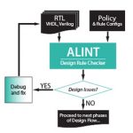
Aldec has a neat tool that should place everyone on the same page within a team. Cowboys beware, this is not for you and you may find yourself at another ranch, move over Hoss. The tool is called ALINT. It is a VHDL/Verilog design rule checker. I know, it does not sound glamorous but let’s face it, the steps to successful design if often not to glamorous.

So let’s walk thru a real example. Say you are the team leader or product team lead for the firmware part of a surveillance RADAR. You are responsible for the beamformer, pulse-compressor, doppler filter. The requirements are traced and you get 6 guys and/or gals for the firmware design of the FPGAs. Two people per function. Now, unguided your beamformer VHDL/Verilog will look very different from the doppler or pulse-compressor teams. For the FPGA clock, some may call it clk, Clock, clk_p. Reset may be called rstn, nrst, rst… Signal names may be a crap shoot. Some folks on the team may use state machines that have the ‘others’ clause, some may use every state. Some may use synchronous reset, some asynchronous, other’s using none assuming default to ‘0’ state. Now each design may simulate correctly and verified against a golden set of data generated by our good ole Octave (You thought I was going to say MATLAB… ok MATLAB too). So what is the issue? All the designs worked in simulation, and let each code their own style and way, why cramp their style? What kind of team leader do we have here? Quick call HR!

The problems, I can almost guarantee will arise during the best part of FPGA design, system integration. Having a common set of VHDL/Verilog design rules such as naming conventions, coding styles, state machine, reset, clocking, signal types… would go a long way on simplicity of debugging and finding errors that would not show up in RTL simulation but in integration such as that ‘Random’ word that is dropped every 14.6 seconds. The other benefit is anyone else can pick up the same code and understand it. How many times has that happened to you? You get the design thrown over the wall from another designer and yikes! You almost have to start from scratch.

There are many more benefits of ALINT such as custom rule creation, phase based linting (you cannot get to the next step until the simplest of warnings are fixed), DO-254/ED-80 support… Check out the tool over at Aldec, and give it a try. I truly wish I had a tool like this years ago!

lang: en_US


Five Things You Don’t Know About MunEDA

Five Things You Don’t Know About MunEDA
by Paul McLellan on 06-17-2014 at 3:00 pm

So first the one thing that you do know. MunEDA are based in Munich which makes them German. I have to confess that until I got involved helping them a bit with some marketing stuff that that was about all I knew about them too.

So now five things that you might not know:

1. MunEDA have a much wider customer list that you know and would even expect. Partially this is because most of their customers are outside the US, largely in Asia. But they are silicon proven by global customers in wireless, memory, automotive, communication, industry, IP and others. Their tools are used by 10 of the top 20 semiconductor companies. Altera is a noteworthy US customer.


2. MunEDA run annual user group meetings in both Europe and Asia with extensive presentations from leading edge customers. These are then archived for their customers as a reference. They have been doing this for years so now there are literally hundreds of presentations by users on how to use MunEDA’s tools effectively.

3. One of MunEDA’s areas of expertise is in variation analysis. This is a growing problem but took a step up in complexity at 20nm with double patterning. The two patterns are not self-aligned so depending on whether the gap between two lines is the minimum or the maximum can make a big different to the performance. Variability is only getting worse with each process node too. MunEDA have the only functional and silicon proven ultra high sigma yield analysis method for 6=9 sigma. To infinity and beyond. Ultra High sigma variation analysis is one of the primary uses that Altera is making use of MunEDA’s tools. Other areas that MunEDA excels in, low power consumption, optimizing circuits for performance enhancements and statistical circuit analysis.


4. One of the next big problems that you haven’t paid enough attention to? Aging and reliability analysis. The smartphone SoC market has made us all lazy since we throw our phones away faster than the chips age or fail. But automotive, aerospace, health and medical. They are all on their way. People get really upset if their cars don’t last fifteen years or more. And those chips are not in such a benign environment as your pocket or purse. They are under the hood where it is hot and vibrating a lot (or, if you go to Canada, cold). And medical? It really ruins your day if you have to have your chest opened to have your heart pacemaker replaced. MunEDA have aging an reliability analysis tools to address all this stuff and proven in silicon.

5. MunEDA is privately held and profitable. They just brought Pete Hansen on board to run their US operations and extend their success in the rest of the world to the US market too. Pete was my VP sales when I was CEO of Envis and then went on to get Solido into many flagship accounts.


More articles by Paul McLellan…


Xilinx KCU105 Evaluation board is key for your demo

Xilinx KCU105 Evaluation board is key for your demo
by Luke Miller on 06-16-2014 at 5:34 pm

I love God, my wife, kids, and FPGA boards. I know I am not alone, there are other nerds out there, don’t be shy. Friday my “Kintex® UltraScale™ FPGA KCU105 Evaluation Kit” came in. Think about this, this is real 20nm Xilinx FPGA hardware that really works. Below is a nice picture of all the swizzles the board has.

I believe this is the first 20nm FPGA board available. I know, this board is obviously lacking an rs-232 port. I hate going thru the USB. I’m old fashioned. My favorite interface is anything fiber. I love fiber, and could be the spokesperson for Metamucil. Anytime I use these boards, I usually use fiber protocols such as VITA17.1/.2 or Fiber Channel. Some of you may pop the card into your PC and use PCIe. Some may use Ethernet, others USB. The point is the KCU105 handles all your interface demands.

The FMC expansion site, FMC1 will quickly let you integrate advanced new standards such as JESD204B, or an x8 Hybrid memory cube. Need memory? DDR4 is on board, already pinned out, ready to be accessed. Flash memory is also available to meet the needs of you that need coefficients or stored data to remain when the power goes off. The heart of this board is the XCKU040 in a -2 Speed Grade. That -2 speed grade means you can run the DSP at 661 MHz, it has 1920 DSP for a potential 2.5 TMACS, not bad!

Me being a RADAR fella, I plan to start playing with some algorithms using MATLAB, coding some C, using Vivado HLS and seeing what I can do. Times have really changed for me in two major areas with FPGA design. Back in the early days, I would have to wait for a custom board to come back, get tested and verified, and then I could test out all my hand written VHDL on the board. I must say this process was not smooth and seemed to make management very cranky. Today I can have my design ready and a Xilinx board around the same time to get near instant gratification. With less errors using Vivado HLS and IP Integrator, as I am no longer hand coding nor using custom CCA’s. Those of you that must have custom needs, and that is many of you, say for some anti-tamper requirements can still use the KCU105 evaluation board. It will allow you to verify your design with all the interfaces you need. When the custom board comes in, you have 99% confidence that if things are no worky, then the issues are perhaps on the custom hardware side. But remember it’s never the software guys 😉

Another trend I am seeing is very aggressive demo/design schedules. It seems that the end customer is not so interested in documents and power point but working demo hardware. Having this board for your demo could be the difference of winning or losing a bid. Xilinx is well aware of this, as I have one of the KCU105 board sitting on my desk. The question is will you have one? Expect availability by the end of the year and shipping in Jan 2015.

lang: en_US


National Semiconductor Education in the Cloud

National Semiconductor Education in the Cloud
by Paul McLellan on 06-16-2014 at 1:28 am

“I wandered lonely as a cloud,” wrote Wordsworth. Well, clouds are pretty lonely in EDA these days. Despite some of the advantages on paper that mean that companies from salesforce.com to Netflix make heavy use of cloud-computing, semiconductor design has barely touched the cloud. One exception was Nimbic (acquired by Mentor last month).

There are many reasons, and there have been several discussions about this already on semiwiki. The biggest ones to my mind are:

  • security: big fabless (and IDM for that matter) companies have policies in place that their intellectual property does not leave the premises. Every time there are reports in the press that passwords have been stolen or other breaches, those policies only get stricter
  • all or nothing: the data volumes involved in designs are so large that either the whole design is done in the cloud or none of it is. It is not really feasible to move designs back and forth. Plus trying toe maintain a design environment in the cloud that is identical to the one locally hosted is a herculean task
  • commercial terms: to get everything into the cloud requires cooperation with the EDA companies on the terms of licenses, and this hasn’t been worked out yet. If you are going to have computing on demand you also need EDA licenses on demand.
  • status quo. the companies who might be expected to dip a toe in the water already have internal CAD groups, internal farms, EDA contracts and adding a few percent of additional cloud resource just adds problems

Instead, the place to start experimenting with the cloud is somewhere that doesn’t have any of these problems:

  • no massive IP issues so no massive security concerns
  • no existing infrastructure so can get going with a cloud-only approach
  • no commercial terms required
  • no status quo so can start from scratch

Sounds too good to be true. But it turns out there is somewhere just like that. Universities in countries that don’t really have very much in the way of IC design infrastructure. But universities don’t really have any money so you can’t just go to the universities and sell them a cloud solution.


However, “Nation building” countries such as Singapore, Malaysia, Saudi Arabia, Morocco, Egypt, Brazil, Vietnam, Pakistan have all targeted IC design as a way to move to a knowledge-based economy, move up the value chain and increase per-capita income. They all have government institutions charged with making things happen in this area. With budgets. Today, although these countries all wonder how to get an Intel or equivalent to set up a group there by tweaking tax policy, the reality is that without designers you can’t pay them to go there. Their big weakenss is that their countries don’t graduate enough designers, dozens rather than hundreds or thousands.

Silicon Cloud International has been targeting these institutions with the proposal to set up a complete cloud-based design environment. They will be the CAD organization for the entire academia of these countries. Instead of being paid by the universities (and in these countries they have even less money than in the US or Europe) they are paid by the institutions charged with getting things going. If they graduate lots of designers then there is scope for locally-based entrepreneurs doing things, or for established semiconductor companies to set up design groups there.


The SCI environment includes all the tools from all the usual suspects (who supply them for free). IP and PDKs are all there too. To address security issues they do something that sounds insane at first. You can neither upload nor download anything. As long as the designs are completely created in the SCI environment then there is no need for it. They already have an agreement with MOSIS so you can tape out without requiring to download anything.

To further address security and IP issues, the cloud based design environment can only be accessed through a Chrome-based thin client. After all, very little local computing power is needed, this is cloud-based. There is not even local storage. The clients cost around $200.


Universities in places like the US are also interested but for different reasons. They are perfectly capable of maintaining their own design environment but it doesn’t really add any value to the university for either teaching or research to do so, it is pure overhead.

What stage are they? The prototype has been active since September last year and a pilot program will start late July.

“All at once I saw a crowd,” Wordsworth continued, “a host of golden daffodils.” Well SCI are hoping to host their own crowd…but of students not daffodils.

More information on SCI’s website here.


More articles by Paul McLellan…


Product Marketing & the Butterfly Effect

Product Marketing & the Butterfly Effect
by Randy Smith on 06-15-2014 at 7:00 pm

I often feel that product marketing can simultaneously be an underrated and overrated function. More often than not, it suggests product goals, pricing, and positioning. Then the marketing department must defend those positions to both engineering and sales. However, both the engineering and sales departments can claim expertise for technology, purchasing patterns and customer desires. In my view, this is the difference between success and failure in the product marketing function – becoming a part of a successful well-integrated team. Product marketing should be a uniting force inside the company. Failure to bring in all voices and enabling enlightened decisions can have huge unexpected results.

When we founded Tangent Systems, I was an engineer. It was the extreme generosity of my co-founders that enabled me to also pursue an MBA at Santa Clara University while we were building Tangents initial products. I didn’t take a full course load, which enabled me to have the best chance to keep pace with my engineering and management responsibilities. When I did complete the MBA, I moved into product marketing, a natural transition for someone with a BSEE and an MBA. Eight months later, Tangent was acquired by Cadence, its very first acquisition. The deal closed in January 1989.

Tangent had two primary place and route products: TANCELL, a channel router-based tool that was the first timing-driven tool on the market; and TANGATE, one of the first commercial area routers. At the time of the acquisition of Tangent, Cadence already had two other channel routers, Symbad from ECAD, and Edge Place & Route by SDA. As Cadence had been formed only recently by the merger of these two companies, there were four product marketing directors – two each from SDA and ECAD. Rod Dudzinski and I, the two product marketing people from Tangent, were assigned to positions which kept us out of the process of deciding what to do with the collection of channel routing products. Bruce Bourbon, Cadence’s Executive VP of Marketing gave me the opportunity to work on product marketing of Design Framework II, as well as participate in all four strategic planning committees. It was not an unreasonable decision under the circumstances, and I have nothing but gratitude for the way that Bruce has mentored me over the years.

Ultimately the decision was made to go forward with Edge Place & Route as it was the only tool integrated in the Cadence Framework. This really amounted to an engineering view of the product. In fact, a deeper analysis of the customer base would have revealed that TANCELL customers were focused on ease-of-use and Edge Place & Route customers were the polar opposite, as they wanted detailed control and integration of the editor. These were two different markets, ASIC standard cell, and structured custom design. The insular approach to product marketing at that time missed this key market reality.

In 1991, Eric Cho, a marketing director not involved in place & route, left Cadence as one of the co-founders of ARCSYS. The first ARCSYS product was ArcCell which clearly targeted the former (and some diehard current) TANCELL customers. This opening made it possible for ARCSYS to gain traction. In time, Gerry Hsu would leave Cadence beginning what was termed “probably the most dramatic tale of white-collar crime in the history of Silicon Valley” by BusinessWeek. Avant! went public, based on a valuation significantly derived on stolen source code. The cash from the IPO allowed Avanti! execute a string of mergers. In 2002, Synopsys bought Avant! and settled the long running lawsuit with Cadence for $265M.

In the end, Synopsys had acquired so many successful product lines through its acquisition of Avant! that it briefly surpassed Cadence as the overall EDA revenue leader in fiscal 2003, and then moved to its current leadership position by 2008. Some of the dip in revenue by Cadence under the Fister regime might be attributable for this, but Cadence’s latest rise is a credit to Lip-Bu Tan’s leadership.

While Synopsys’ long steady increase in revenue is a bi-product of Aart DeGeus’ pragmatic mentality, there is little doubt that the Butterfly Effect of a small product marketing decision at Cadence in 1989 ultimately led to the Synopsys surge after the Avant! acquisition in 2002. Product Marketing decisions are critically important, even the seemingly little or obvious ones.

lang: en_US


FinFET Based Designs Made Easy & Reliable

FinFET Based Designs Made Easy & Reliable
by Pawan Fangaria on 06-15-2014 at 11:00 am

Although semiconductor manufacturing has taken off with FinFET based process technology which provides lucrative payoffs on performance improvement, power reduction and area saving in devices for high density and high performance SoC demand of modern era, apprehensions remain about its reliability due to reduced noise margin, EM and ESD tolerance, and increased heat generation. The increased level of switching due to high density of circuit at higher peak currents and higher grid impedances lead to higher voltage drops, and that combined with reduced supply voltages affects both noise margin and power significantly. The increased voltage drop heightens temperature and thus affects EM reliability of devices as well as interconnects. The FinFET technology also exhibits poor diode protection and that coupled with reduced interconnect reliability can render the chip vulnerable to ESD issues.

So, how to tackle these issues in order to avail the nonpareil advantages of FinFETs? I like Ansys’snew offerings in its RedHawk 2014 platform. My sincere appreciation for Ansys’s effort to proliferate the learning about the real challenges of FinFET technology and how to use RedHawk 2014 to estimate, measure and analyze various parameters to sign-off the semiconductor design at full-chip and package (including 3D stacks) level for power, noise and reliability with silicon correlated accuracy, pico-second resolution and maximum sign-off coverage.

After an overwhelming response to Ansys’s presentation on RedHawk 2014 capabilities to analyze and sign-off FinFET based designs in DAC, they are now unveiling a free webinarfor a larger audience across the world which will provide details about the challenges involved in FinFET based designs and amid those challenges how to address power, noise and reliability sign-off by using RedHawk 2014. The webinar will also provide information about RedHawk certification for 22nm, 16nm and 14nm FinFET processes from multiple foundries.

The new attractions are DMP (Distributed Machine Processing) providing major capacity and performance boost for billion transistor designs including multiple IPs, CPA (Chip-Package Co-Analysis) providing accurate power integrity and reliability analysis including the package impact on die, and temperature-aware EM methodology.

The above image provides a glimpse of package impact analysis on DvD (Dynamic Voltage Drop) with RedHawk-CPA; it considers distributed parasitic network with pin-to-pin mapping.

There are powerful connectivity checks which can determine grid and design weaknesses including power/ground balance, resistance issues, missing vias, static IR, high power density, placement of pads, switches and so on.

The robust reliability checks include power and signal electromigration, chip and system thermal modeling, ESD, clamp placement, cross domain, current density and so on.

The power & noise sign-off includes package-aware chip simulation and chip-aware package simulation with multi-domain power up/down analysis. The vector, vectorless and mixed-excitation analyses are done to improve sign-off coverage along with accuracy. Timing hotspots are also analyzed along with the DvD map.

To know details about these technologies and methodologies, it’s worthwhile attending the webinar. Here is the schedule –

Date: Wednesday, Jun 25[SUP]th[/SUP] 2014
Time: 11:00 AM PDT
Register here to reserve your valuable time and participation in the webinar.

I am excited to hear Calvin Chow, Area Technical Manager at Ansys-Apache, who will provide a great insight into FinFET technology challenges, various tools within the RedHawk 2014 platform and their capabilities to address the reliability of semiconductor designs with FinFETs within the realm of these challenges. Stay tuned to hear more on this.

More Articles by Pawan Fangaria…..

lang: en_US


SemiWiki is an Open Forum for Semiconductor Professionals!

SemiWiki is an Open Forum for Semiconductor Professionals!
by Daniel Nenni on 06-15-2014 at 10:05 am

Why should you be a part of SemiWiki? Two reasons: One, SemiWiki is an excellent semiconductor networking tool. Quite often “who you know” comes into play in your professional life so network-network-network. Two, SemiWiki is all about personal branding. Establish yourself as a person of interest in your chosen field and opportunities will come to you, absolutely.

Today everything and everyone is connected and crowd sourced. In fact, all social media, from blogs, to forums, and wikis have a profound impact on how people communicate, search for information, and make decisions.

If you are a SemiWiki member you can blog, start forum discussions, create wikis, post events to the calendar, send private emails to other members, etc… As an example, the SemiWiki calendar is a high traffic area. When you post an upcoming event your picture and a link to your profile appears with it for all to see. Seriously, I get stopped quite frequently with a, “Hey you are one of the SemiWiki guys!”

Another example is wikis. The most popular wiki contributed by a member has been viewed more than 37k times. This list is a compilation over many years of mergers and acquisitions in the EDA market. The original compilation was done by an individual (Ian Getreu) and is not an official list associated with any company or organization:

A Compilation of EDA Company Merger Listing All the Logos an EDA Company Owns

As a SemiWiki Member you may adopt a screen name to protect your identity but you must register with real names and your LinkedIn profile. Only semiconductor professionals with LinkedIn profiles qualify as SemiWiki Members and all Member information will be held in the strictest confidence. SemiWiki does NOT rent, sell, or trade member information.

Branding works best when you use your real name but that is your choice. I started blogging five years ago and have found it to be an incredible experience. It was rough going in the beginning. In fact I cringe when I look back at some of my first blogs. Fortunately, over the years we have developed a blogging recipe and we would be happy to share it with you. It is a bit of work but at the end of the day you will find writing to be a mind expanding experience, absolutely. And if writing a book is on your bucket list blogging is a great start!

While Google, Yahoo, Bing, and other search engines will continue to play an important role in social media, KNOWLEDGE SHARINGsites like SemiWiki are the new search. The role of user generated content has changed the way information is exchanged. SemiWiki brings technology and technologists closer together than ever before, providing in-demand content and facilitating peer-to-peer communications using Web 2.0 technologies.

User generated content through open collaboration is also called conversational media. In the case of SemiWiki it includes more than one million semiconductor professionals and people interested in the semiconductor industry collaborating around the world. SemiWiki also works closely with more than 40 companies in the fabless semiconductor ecosystem and that means access. Just imagine the possibilities…

More Articles by Daniel Nenni…..


Sensor Hub and Wearable Gestures

Sensor Hub and Wearable Gestures
by Paul McLellan on 06-13-2014 at 10:00 am

One of the challenges with the internet of things (IoT) is that many devices are both always on and battery powered (and not with a large battery). The responsibilities need to be split so that the device senses when it needs to wake up without requiring the application processor to be waking up all the time to make the decision since that would rapidly use up all the available battery power.

Quicklogic last week made two announcements, one a sensor hub for wearables and the other specific gesture algorithms especially for watch like devices worn on the wrist. Two gestures that are important are tapping on the device (like you do with a FitBit for example) or rotating your wrist to wake (basically, looking at the display on the watch should wake up the device so that it displays something).


QuickLogic Corporation announced the immediate availability of its S1 Wearables Sensor Hub, an ultra-low-power, context-aware sensor hub optimized for next-generation wearable applications. QuickLogic’s complete, out-of-the-box solution speeds time-to-market for OEMs developing next-generation wearable applications, particularly in the health and fitness space.

The sensor supports specific contexts for Walking, Running, Cycling, In-Vehicle, On-Person, Not-on-Person. It also supports pedometer functions with separate step-counts for walking and running. It consumes less that 250 microwatts of active power. Offloading the real-time, always-on computation to QuickLogic’s sensor hub enables reduced overall system power, thus extending battery life.

They also announced the immediate availability of its new wearable-specific sensor hub gesture algorithms. Delivering long battery life is critical for wearable devices. QuickLogic’s “Tap-to-Wake” and “Rotate-Wrist-To-Wake” algorithms enable wearable devices to respond to user movements and gestures without waking up the power-hungry host application processor or microcontroller. The algorithms were developed internally by QuickLogic, and provide its OEM customers with a quick and easy method of implementing wearable-specific gestures using QuickLogic’s ultra-low-power, patent pending sensor hub technology.


I think we will see more and more of this sort of part, a little chip that goes along with the rest of the system to make the decision that it is time to wake up or not. Voice recognition is another area where obviously you want to be able to make the decision to wake up or not without requiring a complete voice analysis by the main microprocessor of every sound the microphone picks up.

More information here.


More articles by Paul McLellan…


SEMICON West 2014 Event Calendar

SEMICON West 2014 Event Calendar
by Daniel Nenni on 06-13-2014 at 8:00 am

SEMICON West is the flagship annual event for the global microelectronics industry. It is the premier event for the display of new products and technologies for microelectronics design and manufacturing, featuring technologies from across the microelectronics supply chain, from electronic design automation, to device fabrication (wafer processing), to final manufacturing (assembly, packaging, and test). More than semiconductors, SEMICON West is also showcase for emerging markets and technologies born from the microelectronics industry, including micro-electromechanical systems (MEMS), photovoltaics (PV), flexible electronics and displays, nano-electronics, solid state lighting (LEDs), and related technologies.

[TABLE] style=”height: 640px”
|-
| valign=”top” style=”width: 25%” |
|
|-
| colspan=”2″ valign=”top” style=”width: 25%” | Monday, July 7, 2014
|-
| valign=”top” style=”width: 25%” |
|
|-
| valign=”top” style=”width: 25%” | 9:00am-5:00pm
| SEMI PV Advanced Manufacturing Forum
InterContinental Hotel San Francisco
|-
| valign=”top” style=”width: 25%” |
|
|-
| valign=”top” style=”width: 25%” | 10:30am-12:30pm
| Sustainable Manufacturing Forum:
Session 1 – Sustainable Regulatory Compliance: USA & Europe
San Francisco Marriott Marquis
|-
| valign=”top” style=”width: 25%” |
|
|-
| valign=”top” style=”width: 25%” | 12:30pm-6:00pm
| Imec Technology Forum US (by invitation only)
San Francisco Marriott Marquis
|-
| valign=”top” style=”width: 25%” |
|
|-
| valign=”top” style=”width: 25%” | 1:00pm-5:30pm
| SEMI/Gartner Market Symposium
San Francisco Marriott Marquis
|-
| valign=”top” style=”width: 25%” |
|
|-
| valign=”top” style=”width: 25%” | 1:30pm-3:30pm
| Sustainable Manufacturing Forum:
Session 2- Sustainable Compliance: Asia

San Francisco Marriott Marquis
|-
| valign=”top” style=”width: 25%” |
|
|-
| valign=”top” style=”width: 25%” | 4:00pm-6:00pm
| Sustainable Manufacturing Forum:
Session 3 –
Sustainable Materials Procurement
San Francisco Marriott Marquis
|-
| valign=”top” style=”width: 25%” |
|
|-
| valign=”top” style=”width: 25%” | 6:00pm-7:30pm
| SEMI VIP Reception
San Francisco Marriott Marquis, Atrium
|-
| valign=”top” style=”width: 25%” |
| valign=”middle” |
|-
| colspan=”2″ valign=”top” style=”width: 25%” | Tuesday, July 8, 2014
|-
| valign=”top” style=”width: 25%” |
|
|-
| valign=”top” style=”width: 25%” | 9:00am-9:45am
| Opening Keynote
Mr. Mark Adams, President, Micron
Keynote Stage, Moscone Center, North Hall, Room 135
|-
| valign=”top” style=”width: 25%” |
|
|-
| valign=”top” style=”width: 25%” | 9:00am-12:00pm
| STS Session: Challenges, Innovations and Drivers in Metrology
Session Partner: SEMATECHMoscone North, Hall E, Room 130
|-
| valign=”top” style=”width: 25%” |
|
|-
| valign=”top” style=”width: 25%” | 9:00am-12:00pm
| STS Session: Mobility and More–The M&Ms of Cost Beneficial Advanced Packaging
Session Partner: CPMT
Moscone North, Hall E, Room 131
|-
| valign=”top” style=”width: 25%” |
|
|-
| valign=”top” style=”width: 25%” | 9:45am-10:00am
| Opening Ceremonies
Keynote Stage, Moscone Center, North Hall, Room 135
|-
| valign=”top” style=”width: 25%” |
|
|-
| valign=”top” style=”width: 25%” | 10:00am-5:00pm
| SEMICON West 2014 Exhibition Hours
|-
| valign=”top” style=”width: 25%” |
|
|-
| valign=”top” style=”width: 25%” | 10:30am-12:30pm
| Sustainable Manufacturing Forum:
Session 4 –
Environmental Footprint Assessment
Moscone North Hall, Room 124
|-
| valign=”top” style=”width: 25%” |
|
|-
| valign=”top” style=”width: 25%” | 10:30am-12:45pm
| Next Generations MEMS
TechXPOT South, South Hall
|-
| valign=”top” style=”width: 25%” |
|
|-
| valign=”top” style=”width: 25%” | 10:30am-12:30pm
| Testing into the Future
Hosted by the Collaborative Alliance for Semiconductor Test (CAST)
TechXPOT North, North Hall
|-
| valign=”top” style=”width: 25%” |
|
|-
| valign=”top” style=”width: 25%” | 12:00pm-1:30pm
| STS Sessions Networking Lunch
Moscone North, Hall E, Room 133
|-
| valign=”top” style=”width: 25%” |
|
|-
| valign=”top” style=”width: 25%” | 1:00pm-4:00pm
| Silicon Innovation Forum Conference
Keynote Stage, Moscone Center, North Hall
|-
| valign=”top” style=”width: 25%” |
|
|-
| valign=”top” style=”width: 25%” | 1:30pm-3:00pm
| Sustainable Manufacturing Forum:
Session 5 –
Green House Gass (GHG) Assessment
Moscone North Hall, Room 124
|-
| valign=”top” style=”width: 25%” |
|
|-
| valign=”top” style=”width: 25%” | 1:30pm-4:45pm
| STS Session:Yield Session: Defectivity and Process Variability-Inspection, Defect Reduction Challenges and Process Controls at the Sub 20nm Nodes
Session Partner: SEMATECH
Moscone North, Hall E, Room 130
|-
| valign=”top” style=”width: 25%” |
|
|-
| valign=”top” style=”width: 25%” | 1:30pm-4:30pm
| STS Session: Embracing what’s NEXT – Devices & Systems for Big Data, Cloud and IoT
Moscone North, Hall E, Room 131
|-
| valign=”top” style=”width: 25%” |
|
|-
| valign=”top” style=”width: 25%” | 1:30pm-3:30pm
| Variability Control–A Key Challenge and Opportunity for Driving Towards Manufacturing Excellence
Session Partner: SEMATECH TechXPOT South, South Hall
|-
| valign=”top” style=”width: 25%” |
|
|-
| valign=”top” style=”width: 25%” | 1:30pm-3:30pm
| Speeding on the Roadmap-The Future of 3D NAND Flash
Hosted by: SEMI Chemical and Gases Manufacturers Group (CGMG)
TechXPOT North, North Hall
|-
| valign=”top” style=”width: 25%” |
|
|-
| valign=”top” style=”width: 25%” | 3:30pm-5:00pm
| Sustainable Manufacturing Forum:
Session 6-
Advanced Abatement Systems
Moscone North Hall, Room 124
|-
| valign=”top” style=”width: 25%” |
|
|-
| valign=”top” style=”width: 25%” | 4:00pm-6:00pm
| Silicon Innovation Showcase and Reception
Moscone North Hall, Room 134
|-
| valign=”top” style=”width: 25%” |
|
|-
| valign=”top” style=”width: 25%” | 4-30pm-7:30pm
| Connect with India – The Next Semiconductor Manufacturing Region
San Francisco Marriott Marquis
|-
| valign=”top” style=”width: 25%” |
|
|-
| valign=”top” style=”width: 25%” | 5:00pm-8:00pm
| Leti Day (By Invitation Only)
W Hotel
|-
| valign=”top” style=”width: 25%” |
|
|-
| colspan=”2″ valign=”top” style=”width: 25%” | Wednesday, July 9, 2014
|-
| valign=”top” style=”width: 25%” |
|
|-
| valign=”top” style=”width: 25%” | 7:30am-10:00am
| Sokudo Lithography Breakfast Forum 2014
San Francisco Marriott Marquis
|-
| valign=”top” style=”width: 25%” |
|
|-
| valign=”top” style=”width: 25%” | 7:30am-9:00am
| SEMI Membership Breakfast and Announcement of the Board
(Members Only)

San Francisco Marriott Marquis
|-
| valign=”top” style=”width: 25%” |
|
|-
| valign=”top” style=”width: 25%” | 8:00am-6:30pm
| Global Summit for Advanced Manufacturing (Day 1 of 3)
San Francisco Marriott Marquis
|-
| valign=”top” style=”width: 25%” |
|
|-
| valign=”top” style=”width: 25%” | 9:00am-12:00pm
| STS Session: Design for Test
Session Partner: Electronic Design Automation Consortium
Moscone North, Hall E, Room 130
|-
| valign=”top” style=”width: 25%” |
|
|-
| valign=”top” style=”width: 25%” | 9:00am-12:00pm
| STS Session: Getting to 5nm Devices: Evolutionary Scaling to Disruptive Scaling and Beyond
Moscone North, Hall E, Room131
|-
| valign=”top” style=”width: 25%” |
|
|-
| valign=”top” style=”width: 25%” | 10:00am-10:45am
| Keynote:
Mr. Sanjay Ravi
Worldwide Managing Director, Discrete Manufacturing Industry
Microsoft Corporation
Keynote Stage, Moscone Center, North Hall, Room 135
|-
| valign=”top” style=”width: 25%” |
|
|-
| valign=”top” style=”width: 25%” | 10:00am-5:00pm
| SEMICON West 2014 Exhibition Hours
|-
| valign=”top” style=”width: 25%” |
|
|-
| valign=”top” style=”width: 25%” | 10:30am-12:00pm
| Sustainable Manufacturing Forum:
Session 7-
Energy/Resource Conservation
Moscone North Hall, Room 124
|-
| valign=”top” style=”width: 25%” |
|
|-
| valign=”top” style=”width: 25%” | 10:30am-12:30pm
| Subcomponent Supply Chain Challenges for 10 nm and Beyond
Hosted by: SEMI Semiconductor Components, Instruments, and Subsystems Special Interest Group
TechXPOT South, South Hall
|-
| valign=”top” style=”width: 25%” |
|
|-
| valign=”top” style=”width: 25%” | 10:30am-12:30pm
| Bringing Silicon Photonics to Market
TechXPOT North, North Hall
|-
| valign=”top” style=”width: 25%” |
|
|-
| valign=”top” style=”width: 25%” | 12:00pm-12:30pm
| Sustainable Manufacturing Forum:
Session 8-
Sustainable Technologies Award
Moscone North Hall, Room 124
|-
| valign=”top” style=”width: 25%” |
|
|-
| valign=”top” style=”width: 25%” | 12:00pm-1:30pm
| STS Sessions Networking Lunch
Moscone North, Hall E, Room 133
|-
| valign=”top” style=”width: 25%” |
|
|-
| valign=”top” style=”width: 25%” | 1:30pm-4:30pm
| STS Session: Readiness of Advanced Lithography Technologies for HVM
Moscone North, Hall E, Room 131
|-
| valign=”top” style=”width: 25%” |
|
|-
| valign=”top” style=”width: 25%” | 1:30pm-3:00pm
| Sustainable Manufacturing Forum:
Session 9-
Next Generation Eco Fab, Part 1
Moscone North Hall, Room 124
|-
| valign=”top” style=”width: 25%” |
|
|-
| valign=”top” style=”width: 25%” | 1:30pm-4:30pm
| Wafer Geometry Control for Advanced Semiconductor Manufacturing
San Francisco Marriott Marquis
|-
| valign=”top” style=”width: 25%” |
|
|-
| valign=”top” style=”width: 25%” | 1:30pm-3:30pm
| Secondary Equipment for Mobile & Diversified Applications
Hosted by the Secondary Equipment and Applications Americas Chapter
TechXPOT South, South Hall
|-
| valign=”top” style=”width: 25%” |
|
|-
| valign=”top” style=”width: 25%” | 1:30pm-3:35pm
| Driving Automotive Innovation-The Enabling Role of Semiconductor and IC Packaging
Session Partner: MEPTEC
TechXPOT North, North Hall
|-
| valign=”top” style=”width: 25%” |
|
|-
| valign=”top” style=”width: 25%” | 1:30pm-5:00pm
| Test Vision 2020 Workshop and reception (Day 1 of 2)
Moscone North, Hall E, Room 130
|-
| valign=”top” style=”width: 25%” |
|
|-
| valign=”top” style=”width: 25%” | 3:30pm-5:00pm
| Sustainable Manufacturing Forum:
Session 10 –
Next Generation Eco Fab, Part 2
Moscone North Hall, Room 124
|-
| valign=”top” style=”width: 25%” |
|
|-
| valign=”top” style=”width: 25%” | 4:00pm-5:30pm
| Bulls and Bears
W Hotel
|-
| valign=”top” style=”width: 25%” |
|
|-
| colspan=”2″ valign=”top” style=”width: 25%” | Thursday, July 10, 2014
|-
| colspan=”2″ valign=”top” style=”width: 25%” |
|-
| valign=”top” style=”width: 25%” | 7:30am-10:00am
| Entegris Yield Breakfast Forum 2014
San Francisco Marriott Marquis
|-
| valign=”top” style=”width: 25%” |
|
|-
| valign=”top” style=”width: 25%” | 8:00am-5:15pm
| Global Summit for Advanced Manufacturing (Day 2 of 3)
San Francisco Marriott Marquis
|-
| valign=”top” style=”width: 25%” |
|
|-
| valign=”top” style=”width: 25%” | 8:00am-5:00pm
| Test Vision 2020 (Day 2 of 2)
Moscone North, Hall E, Room 130
|-
| valign=”top” style=”width: 25%” |
|
|-
| valign=”top” style=”width: 25%” | 9:00am-12:00pm
| STS Session: 450mm Technology Development Update
Moscone North, Hall E, Room 131
|-
| valign=”top” style=”width: 25%” |
|
|-
| valign=”top” style=”width: 25%” | 10:00am-4:00pm
| SEMICON West 2014 Exhibition Hours
|-
| valign=”top” style=”width: 25%” |
|
|-
| valign=”top” style=”width: 25%” | 10:00am-4:45pm
| FlexTech Alliance Workshop: Flexible Hybrid Electronics for Wearable Applications – Challenges and Solutions
San Francisco Marrriott Marqui
|-
| valign=”top” style=”width: 25%” |
|
|-
| valign=”top” style=”width: 25%” | 10:30am-12:30pm
| Sustainable Manufacturing Forum:
Session 11 –
Sustainability of Advanced Materials
Moscone North Hall, Room 124
|-
| valign=”top” style=”width: 25%” |
|
|-
| valign=”top” style=”width: 25%” | 10:30am-12:30pm
| 3D Printing: Science Fiction or the Next Industrial Revolution?
Session Partner: SEMICO Research
TechXPOT South, South Hall
|-
| valign=”top” style=”width: 25%” |
|
|-
| valign=”top” style=”width: 25%” | 10:30am-12:30pm
| Disruptive Compound Semiconductor Technologies
TechXPOT North, North Hall
|-
| valign=”top” style=”width: 25%” |
|
|-
| valign=”top” style=”width: 25%” | 12:00pm-1:30pm
| STS Sessions Networking Lunch
Moscone North, Hall E, Room 133
|-
| valign=”top” style=”width: 25%” |
|
|-
| valign=”top” style=”width: 25%” | 1:30pm-3:30pm
| Sustainable Manufacturing Forum:
Session 12 –
Fabless Considerations in Manufacturing
Moscone North Hall, Room 124
|-
| valign=”top” style=”width: 25%” |
|
|-
| valign=”top” style=”width: 25%” | 1:30pm-3:30pm
| STS Session: Breakthrough High Volume Manufacturing:New Paradigms for the Road Ahead
Moscone North, Hall E, Room 131
|-
| valign=”top” style=”width: 25%” |
|
|-
| valign=”top” style=”width: 25%” |
|
|-
| valign=”top” style=”width: 25%” | 1:30pm-3:30pm
| SEMICON West 2014 IoT Startup Showcase – An SK Telecom Americas Innopartners Program
TechXPOT North
|-
| valign=”top” style=”width: 25%” |
|
|-
| valign=”top” style=”width: 25%” | 1:30pm-3:30pm
| Breakthrough Research Technologies
Universities, Industries, Consortiums
TechXPOT South
|-
| valign=”top” style=”width: 25%” |
|
|-
| valign=”top” style=”width: 25%” |
|
|-
| colspan=”2″ valign=”top” style=”width: 25%” | Friday, July 11, 2014
|-
| colspan=”2″ valign=”top” style=”width: 25%” |
|-
| valign=”top” style=”width: 25%” | 9:00am-4:00pm
| Global Summit for Advanced Manufacturing (Day 3 of 3)
Manufacturer’s Tour

|-