BannerforSemiWiki 800x100 (2)

RTL Sign-off – At an Edge to become a Standard

RTL Sign-off – At an Edge to become a Standard
by Pawan Fangaria on 02-01-2014 at 10:00 am


Ever since I have seen Atrenta’s SpyGlass platform providing a comprehensive set of tools across the semiconductor design paradigm, I felt the need for a common set of standards to evolve for sign-off at RTL level. Last December, when I read an EE Times articleof Piyush Sancheti, VP, Product Marketing at Atrenta, where he talks about a billion gate SoC design, shrinking market windows, and design cycles to the level of 3-6 months, I was looking for an opportunity to talk to him in a broader sense on how RTL level design paradigm is proliferating and what we can see in future. This week I had a nice opportunity talking to him face-to-face in Atrenta’s Noida office. Here is the conversation –

Q: SpyGlass is primarily providing a platform for designs at RTL and for sign-off at that stage. What has been your experience so far?

In today’s SoC design environment, you have size, scale and complexity of advanced nodes being the prime factors. Most of the SoCs use several soft IPs, configurable at different levels, and some hard IPs as well. Iterative design closures do not serve the purpose for such large designs. Add to it very short market windows; there is another level of market segment coming up for Internet-of-Things, that has very short turn-around-time in the order of 3 months. RTL sign-off has become a need today to answer this faster design closure with lesser cost.

So, to answer in short, our leading edge customers are executing on RTL sign-off and are happy to see the value in it. Last year was the best year for us in terms of business and growth and we are looking at a bright future from here.

Q: Considering the amount of IP re-use and sourcing from third party for SoC design, a standard RTL sign-off criteria can help in reliable IP exchange as most of the IPs are sourced at RTL level. Your comments?

Yes, definitely, at the top level an SoC can have just connectivity between many IPs connected through glue logic. So, quality of the SoC will depend on the quality of IPs and therefore a standard criterion must be there for IPs, internal or external. We have been working with TSMCon a standard for soft IP qualification.

Q: That’s quite encouraging. Looking at your talk in EE Times about billion gate SoCs becoming a reality, I can definitely see that RTL sign-off is a must. But do you see common standard RTL sign-off criteria or rather RTL coverage factors evolving across the industry for the overall semiconductor design?

Yes, it’s required. Even if all IPs on an SoC are qualified, it doesn’t guarantee the quality of the SoC. What if there is a clocking scheme mismatch between IPs? Even at the connectivity level between IPs, we need to look at the common plane issues, consistency, synchronous versus asynchronous and the like. So, a standard at SoC level sign-off is again a must for the industry. And we are working at it, along with some of our leading customers; it depends on a majority of the design houses adopting this path. It will take time to break that inertia; people will realize that this change in methodology is needed when they are no longer able to continue with the same old methodology.

We have talked about the problems so far, let’s talk about some solutions. We now offer a smart abstract model concept for blocks in SoC design. RTL sign-off can be done at a hierarchical level; this has very fast turnaround. This is now in use in some of the most complex SoC designs with multiple levels of hierarchy. We have seen amazing results in performance, capacity, memory utilization, number of violations etc. We are talking gains that are in one or two orders of magnitude. So, we definitely would be interested in evolving the common standard for SoC sign-off at RTL.

Q: What all should get covered in RTL sign-off?

It’s across various design domains; clocking, testability, physical, timing, area, and power. Rules to avoid congestion and ensure routing completion such as fan-in, fan-out, mux sizes and cell pin density. On the timing side, there is logic depth, CDC, clock gating etc. Similarly there are rules for power and area. We have about 300 rules of the first order. These have broad applicability across a wide range of the market segments.

Q: RTL sign-off is a must at the beginning of an SoC design and a post layout sign-off at the end. Do you see the need for any intermediate level of sign-off such as post floorplan level?

Yes, SoC design needs a continuous monitoring at each stage. Quality and sign-off is a culture which must be exercised at each stage as the SoC passes through the design phases such as floorplan, placement and so on. By doing sign-off at RTL, one can get to design closure much faster, more productively and at lesser cost. As we pass through lower levels of design, the cost and iteration time increases. The other advantage at RTL signoff is that it minimizes iterations at lower levels. Overall it can reduce the design schedule risk by 30-50%.

Q: Do you see a possibility of leading organizations working at RTL, joining together to define a common standard for RTL sign-off of IPs and SoCs for the semiconductor industry? Can Atrenta take a lead? Who should own the standard?

As I said earlier, we are already working with TSMCand some of our other leading customers on this. We would be very interested in a common standard evolution which can benefit the whole semiconductor design industry. However, it needs about 10-12 major players from the design community, foundry and EDA to get the ball rolling. Eventually it will become a success only when majority of the semiconductor design community embraces it, as we have seen in other spaces. At this moment, we are not limited by capability; we are limited by the number of users which need to be large enough to provide that kind of momentum.

So, yes we can give it a start, mature it, but going forward some standard body should own it. It may be a new standard body or any of the existing one, we have to see.

Q: How far from now do you see that standard evolving?

I guess it should take minimum 18-24 months from now. It will not fly until we have a critical mass of the community starting to use it.

I felt extremely happy after talking to Piyush, especially on learning that what I was thinking is already in progress. This was one of my best conversations with industry leads. I really admire Piyush’s thought process when he said, “we are not doing it on our own. We continuously learn from our customers and partners who provide us the right direction to do things better in this challenging environment and change the ways that can lead to better productivity.” Let’s watch what’s there in store for future.

More Articles by Pawan Fangaria…..

lang: en_US


Power and Thermal Modeling Approach for Embedded and Automotive using ESL Tools

Power and Thermal Modeling Approach for Embedded and Automotive using ESL Tools
by Daniel Payne on 01-31-2014 at 7:04 pm

Did you know that an S-class Mercedes Benz can use 100 microprocessor-based electronic control units (ECUs) networking throughout the vehicle that run 20-100 million lines of code (Source: IEEE)?


2014 Mercedes-Benz CLA

Here’s a quick list of all the places that you will find software controlling hardware in an automobile:
Continue reading “Power and Thermal Modeling Approach for Embedded and Automotive using ESL Tools”


How Do You Verify a NoC?

How Do You Verify a NoC?
by Paul McLellan on 01-31-2014 at 6:01 pm

Networks-on-chip (NoCs) are very configurable, arguably the most configurable piece of IP that you can put on a chip. The only thing that comes close are highly configurable extensible VLIW processors such as those from Tensilica (Cadence), ARC (Synopsys) and CEVA but Sonics would argue their NoCs are even more flexible. But this leads to a major challenge: how do you verify one of these beasts.

NoCs are defined by a configuration file. A NoC used to link perhaps a dozen blocks on an SoC but these days there may be a couple of hundred and the configuration file can be tens of thousands of lines long. This leads to the problem: how do you verify that the NoC RTL does indeed correctly represent the functionality defined by the configuration file. A big part of the problem is that everything is configurable. The protocols used, the performance, the connectivity, whether interfaces are blocking or non-blocking, how wide signals are. Everything. They are the Burger Kings of the SoC: have it your way.

The next level down a NoC consists of functional blocks connected by the actual signal buses. So the best approach is hierarchical, verify that each of those functional blocks does what it is meant to do and that they are hooked up correctly.

Like everyone else, Sonics uses constrained random verification, lots of SystemVerilog Assertions (SVAs) along with the constraints to ensure that the random vectors generated are themselves correct. Since the NOC is so configurable, these are not fixed files but also need to be automatically generated from the configuration file that specifies the NoC. Then vectors can be run and, hopefully, none of the SVAs fail (which would point to a problem).

But Sonics also does something other people do not: it also generates a SystemC transactional level model (TLM) corresponding to most blocks. These are still cycle accurate so not necessarily quite what you first think of when you hear TLM. The SystemC model contains protocol checkers (green in the diagram below) along with signal level adapters (light blue) to hook up the reference model. The light blue block on the left is the RTL block being verified.


The protocol checkers are a really important part of the verification environment. These monitor the signals going into and coming out of a block and verify that the protocols are implemented correctly.

Once the NoC is verified, that doesn’t guarantee that it works correctly on the SoC. Interface protocols are a sort of contract and the user’s IP blocks need to keep their side of the bargain. Once again a key part of the verification is the protocol checkers. These will call foul if an interface does not behave in line with the contract.

Sonics recommends that users keep the protocol checkers in place throughout the design process. They do not generate RTL so they don’t get designed into the chip itself. However during any RTL simulation they will catch many problems when they first occur rather than leaving them to show up as an obscure bug, perhaps on the other side of the chip many clock cycles later. In fact the first thing a Sonics AE will ask when a customer tries to report a bug in the NoC is whether the simulation has been run with all the protocol checkers turned on. Many bugs have gone away once this is done. What looked at first like an obscure bug in the NoC itself was actually caused by a completely different block violating the protocol.

The process just described is how to test a particular implementation of a NoC when designing an SoC. But that doesn’t help Sonics themselves check the whole tool chain. So every night they go one step further than constrained random. They generate random NoCs and then run the verification on them long enough to be confident that the implementation is correct. Then they generate another NoC and do it again. All night, every night.


Update on a Space-Based Router for IC Design

Update on a Space-Based Router for IC Design
by Daniel Payne on 01-31-2014 at 11:50 am

When I started my IC design career back in 1978 all IC routing was done manually, today however we have many automated approaches to IC routing that save time and do a more thorough job than manual routing. To get an update on space-based routers for IC design I connected with Yuval Shay at Cadence today. The basic idea behind a spaced-based router is to simultaneously address:
Continue reading “Update on a Space-Based Router for IC Design”


SOI Future or Flop?

SOI Future or Flop?
by Scotten Jones on 01-31-2014 at 8:00 am

Silicon On Insulator (SOI) is a technology that has been in use by the semiconductor industry for a long time. Early technologies such as Silicon On Sapphire (SOS) were reported as early as the sixties. In the eighties technologies such as V groove dielectric isolation were used. In the nineties we saw wafer bonding become the most prevalent technique for SOI fabrication, although implanted oxygen was also in use. It wasn’t until the late nineties that IBM ushered in the modern era of SOI usage for high performance CMOS.

SOI has always offered certain performance advantages with radiation hardness, the ability to isolate both positive and negative voltages on the same substrate and reduced power consumption being a few key examples. Although this article is focused on state-of-the-art CMOS, SOI is also an important part of many emerging Micro Electro Mechanical System (MEMS) applications and some power IC applications as well. The issue with SOI has always been cost and it has always been a niche technology.

In the late nineties IBM introduced Partially Depleted SOI (PDSOI) for high performance CMOS. The introduction of a buried oxide layer under the MOSFET reduced parasitic source/drain (S/D) capacitance reducing power consumption. Planar MOSFETs have highly doped source and drain regions of one conductivity type separated by a lightly doped channel of opposite conductivity type. The surface of the channel is covered with an insulating layer and a gate electrode. The gate of a MOSFET really only has good control of the surface and in the sub surface regions there are S/D leakage paths. With partially depleted SOI, the device silicon layer on top of the insulator is still thick enough that the gate can’t fully deplete the channel in the off-state and leakage paths still exist. PDSOI also requires all of the processing of a standard bulk process plus a couple of SOI specific masks. This coupled with the high cost of SOI substrates yields a very expensive process. In spite of the cost issues, IBM utilized PDSOI from 130nm to 22nm for high performance processors. Concurrently IBM developed a high performance embedded DRAM technology (eDRAM) that took advantage of the buried oxide isolation in SOI making the process ideal for their high performance processors needs. In the early 2000s AMD was a development partner of IBM and they also adopted PDSOI for their processors for the 90nm through 45nm generation and at one point all three major game consoles utilized PDSOI based processors. Today IBM’s 22nm process is to the best of our knowledge the only leading edge logic process still running on PDSOI. In IBM’s case the processors are used for high margin server products and performance is far more important than cost. Other PDSOI users have concluded that any performance advantages are outweighed by the cost.

Fully Depleted MOSFETs

As MOSFET gate lengths have shrunk, S/D leakage has been increasing exponentially and a change in MOSFET architecture is now required with the 20nm node expected to be the end for the bulk – planer MOSFET. If instead of a partially depleted channel the channel of a MOSFET is full depleted in the off-state, S/D leakage is reduced by orders of magnitude. There are two main techniques currently in use for fully depleted MOSFETs, FinFETs and Fully Depleted SOI (FDSOI).

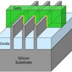
FinFETs utilize thin fins of silicon standing up perpendicular to the wafer surface in a 3D configuration for the MOSFET channel. The fin may have gates on both sides (a classic FinFET) or on both sides and the top (Trigate). With gates on both sides the fin thickness must be approximately one half the gate length to be fully depleted and with gates on both sides and the top the fin width must be less than approximately one times the gate length to be fully depleted. The Trigate configuration relaxes the fin thickness requirements making them easier to manufacture. FinFETs can also be fabricated on either bulk or SOI (more on that later). At 22nm Intel was the first in the industry to introduce FinFETs with their Trigate process. Intel announced at the time that the Trigate process adds 5% to the processing costs versus planar. One interesting observation here is that the FinFET process actually requires fewer masks and process steps than bulk. In an ideal FinFET, the channel would be undoped but in order to achieve multiple threshold voltages multiple gate work function metals would be required. Due to the difficulty of fabricating multiple work function metals, FinFETs today have doped channels and this requires masks and implants for Vt tuning, however the complexity of the Vt tuning scheme is reduced relative to bulk-planar MOSFETs due to the absence of Halos. If you just look at the processing steps for a FinFET versus a bulk-planar MOSFET the FinFET flow is simpler. I believe the added cost is due to yield issues from the fin formation on bulk process where controlling the fin height is very difficult.

The other option for fully depleted MOSFETs is planar FDSOI. In planar FDSOI the device silicon layer thickness on top of the buried oxide must be less than approximately one third the gate length. The challenges of making a sufficiently thin and uniform FDSOI device layer took many years to overcome and FDSOI has only recently become available. There is a very technologically interesting byproduct of such a thin device silicon layer over an insulator. It is possible to fabricate a buried back gate under the MOSFET channel. The back gate can be biased to tune the MOSFET performance and or threshold voltage. Modern System On a Chip (SOC) designs require three or even four threshold voltages. For a 20nm bulk-planar MOSFET technology each threshold voltage requires an NMOS and a PMOS threshold voltage mask and implant. Halo implants also strongly influence threshold voltage and each threshold voltage requires a S/D Ext/Halo mask and set of implants. S/D Ext/Halos require three to four implants each. Tailoring of deep S/D contact implants can also be required. The bottom line is a planar-bulk MOSFET can require 4 to 6 masks and 9 to 15 implants for each threshold voltage! Multiply that number by 3 or 4 threshold voltages and you can see what a huge process and cost driver threshold voltage is. Eliminating all of these masks and implants by biasing a back gate offsets the cost of the SOI starting substrate and yields a cost competitive technology with better performance. For the interested reader I have written a cost analysis comparing FDSOI to bulk at 22nm available here: http://www.icknowledge.com/news/presentations.html (in the spirit of full disclosure the work was funded by SOI producer Soitec).

FDSOI Versus FinFET
Now that we have reviewed the options for fully depleted MOSFETs let’s take a look at the relative merits of the two approaches.

I have spent a lot of time looking at performance of FinFETs versus FDSOI. I believe it is generally acknowledged that FinFETs offer the highest ultimate speed and drive current in the smallest area. FDSOI on the other hand offers lower power and the best performance per watt. This would suggest that for very high performance applications FinFETs would be the best technology. On the other hand if you are designing a SOC IC for a mobile application FDSOI would be a better choice.

There are a number of cost comparisons that have been published of FDSOI versus FinFETs on bulk showing FinFETs are significantly more expensive. Handel Jones of IBS for example has published a 20nm die cost comparison showing a 35% higher wafer cost for FinFETs versus FDSOI. When I look at the specific process steps for a bulk FinFET versus an FDSOI device I don’t see this at all. I can only assume that there are some unfavorable yield assumptions in the FinFFET portion of the analysis. I haven’t spoken to Handel Jones about this but one of my colleges asked him about this at ISS this year and my understanding is that Dr. Jones acknowledged that it was yield driven. I personally find it very hard to believe that after over two years of manufacturing experience on the process, Intel wouldn’t have over 90% wafer yield on their process by now and I therefore believe these higher cost estimates are wrong.

There have also been published analysis from IBM claiming that FinFETs on SOI are cheaper than FinFETs on bulk (although in the same presentation they also appear to acknowledge that after accounting for the more expensive SOI wafer the costs are roughly the same). Based on my own analysis and Intel’s published 5% cost difference at 22nm I believe FinFETs on bulk and FDSOI at the 22nm/20nm node have very similar cost.

I have also looked at 14nm costs for FDSOI, FinFETs on bulk and FinFETs on SOI. The following table summarizes some findings based on a detailed analysis of the processes.

[TABLE] align=”center” border=”1″
|-
| style=”width: 167px; height: 17px” |
| style=”width: 80px; height: 17px” | FDSOI
| style=”width: 90px; height: 17px” | FinFET on bulk
| style=”width: 86px; height: 17px” | FinFET on SOI
|-
| style=”width: 167px; height: 17px” | Mask layers
| style=”width: 80px; height: 17px” | 44
| style=”width: 90px; height: 17px” | 46
| style=”width: 86px; height: 17px” | 43
|-
| style=”width: 167px; height: 17px” | Multi patterning masks
| style=”width: 80px; height: 17px” | 8
| style=”width: 90px; height: 17px” | 13
| style=”width: 86px; height: 17px” | 11
|-
| style=”width: 167px; height: 17px” | Total masks
| style=”width: 80px; height: 17px” | 52
| style=”width: 90px; height: 17px” | 59
| style=”width: 86px; height: 17px” | 54
|-
| style=”width: 167px; height: 17px” | Substrate cost
| style=”width: 80px; height: 17px” | High
| style=”width: 90px; height: 17px” | Low
| style=”width: 86px; height: 17px” | High
|-

The FDSOI mask and cut mask count is based on a STMicro presentation that details the masks for their upcoming 14nm process. The Intel and IBM mask counts are based on my own analysis performed with other industry process experts I work with and include all mask layers required for the full process. In the case of IBM I have removed the eDRAM related masks to create a direct comparison. All three processes are also based on 10 metal layers and 3 threshold voltages. Looking at the mask counts and process details I don’t see a big cost advantage for any of the three processes and don’t believe cost will be the differentiating factor. If anything a straight forward process and materials analysis appears to favor FinFETs on bulk. If any SemiWiki readers believe they understand FinFET processing and disagree with these counts I would be happy to have a private conversation about it. I am also still working on a detailed cost comparison of the three processes but don’t anticipate that will change my conclusions.

What Leading Edge Logic Companies are Doing
To summarize this paper so far, FinFET appears to be the best solution where ultimate performance is the goal with power consumption being a secondary concern and FDSOI appears to be the best solution where power is the primary concern.

We will now examine what companies are actually doing at 14nm. The following table summarizes all of the companies pursuing 14nm logic with their announced process technology.

[TABLE] align=”center” border=”1″
|-
| style=”width: 201px; height: 17px” | Company
| style=”width: 201px; height: 17px” | 14nm technology
|-
| style=”width: 201px; height: 17px” | Global Foundries
| style=”width: 201px; height: 17px” | FinFET on bulk although will also make FDSOI under a manufacturing agreement with ST Micro
|-
| style=”width: 201px; height: 17px” | IBM
| style=”width: 201px; height: 17px” | FinFET on SOI
|-
| style=”width: 201px; height: 17px” | Intel
| style=”width: 201px; height: 17px” | FinFET on bulk
|-
| style=”width: 201px; height: 17px” | Samsung
| style=”width: 201px; height: 17px” | FinFET on bulk
|-
| style=”width: 201px; height: 17px” | ST Micro
| style=”width: 201px; height: 17px” | FDSOI
|-
| style=”width: 201px; height: 17px” | TSMC
| style=”width: 201px; height: 17px” | FinFET on bulk
|-
| style=”width: 201px; height: 17px” | UMC
| style=”width: 201px; height: 17px” | FinFET on bulk
|-

With many years or development and hundreds of million or even billions of dollars invested in process development I would consider the processes in this table to be pretty well locked in at this point.

Looking at this table, FinFET on bulk represents roughly 95% of the expected 14nm capacity with FinFET on SOI and FDSOI only representing about 5%.

Looking at IBM and taking into account their eDRAM on SOI technology, a FinFET on SOI strategy makes perfect sense. IBM needs the highest possible performance plus eDRAM and there is an argument that FinFET on SOI has some performance advantages over FinFET on bulk.

For Intel performance is also a big driver although in recent years they have become more focused on performance per watt than they were previously. FinFETs on bulk make a lot of sense for Intel.

Looking at the major foundries, TSMC, Global Foundries, Samsung and UMC their technology choice is not as easy to understand. The big business driver for the foundries these days is SOCs going into mobile devices where FDSOI would appear to be a better process. I have spent a lot of effort trying to understand this issue. I have discussed this with a lot of knowledgeable industry experts and as best as I can piece together it appears that FDSOI wasn’t ready back when these companies were making technology decisions. There is also a lingering concern about the SOI substrate cost and the availability of enough wafers to service an Intel, TSMC or Samsung.

The bottom line is FDSOI will be in use at ST Micro and some production volume at Global Foundries. IBM will utilize SOI for FinFETs. At 14nm with process development essentially complete, SOI is unlikely to be much more than 5% of production volumes.

10nm and 7nm Forecast

Another interesting question is could SOI increase market share at 10nm or 7nm. I believe 10nm development is pretty well along at this point and companies that have invested so much money and time into FinFETs are unlikely to change after one generation. There is a lot of published work from companies like TSMC on Ge PMOS fins for 10nm and they have even made an announcement that they plan to use Ge PMOS fins at 10nm. Possibly Global Foundries could ramp up FDSOI if they see a lot of demand but I think it is unlikely anyone else would switch.

At 7nm there are differing opinions of the viability of FDSOI. There appears to be a clear path to 10nm FDSOI but 7nm is more controversial. At IEDM in December 2013 there was an FDSOI paper and the authors appeared to be confident 7nm could be achieved (keep in mind that the device layer has to get thinner as the gate length scales down). Other FDSOI experts I have spoken to are less optimistic.

Conclusion
Based on what companies are doing today, the installed and planned capacity for the companies, the likelihood of changes at 10nm and the difficulties of scaling FDSOI to 7nm, I expect the leading edge logic market to look like this:

[TABLE] align=”center” border=”1″
|-
| style=”width: 90px; height: 17px” | Node
| style=”width: 90px; height: 17px” | FDSOI
| style=”width: 97px; height: 17px” | FinFET on bulk
| style=”width: 96px; height: 17px” | FinFET on SOI
|-
| style=”width: 90px; height: 17px” | 14nm
| style=”width: 90px; height: 17px” | 2.1%
| style=”width: 97px; height: 17px” | 96.2%
| style=”width: 96px; height: 17px” | 1.7%
|-
| style=”width: 90px; height: 17px” | 10nm
| style=”width: 90px; height: 17px” | 5.0%
| style=”width: 97px; height: 17px” | 93.5%
| style=”width: 96px; height: 17px” | 1.5%
|-
| style=”width: 90px; height: 17px” | 7nm
| style=”width: 90px; height: 17px” | 1.6%
| style=”width: 97px; height: 17px” | 96.9%
| style=”width: 96px; height: 17px” | 1.5%
|-

SOI clearly has its place in the mobile market and is also gaining a lot of traction in the RF front end of cell phones, but given the current technology and capacity commitments of the leading edge logic producers FDSOI appears likely to peak at only 6.5% of the leading edge logic market.

lang: en_US


Getting the best from MIPI IP Toolbox

Getting the best from MIPI IP Toolbox
by Eric Esteve on 01-31-2014 at 4:07 am

The set of MIPI specifications has severely enlarged during the past year. This is a positive point, as the large set of specifications induces a wider choice, and a chip maker can decide to implement a complex specification to differentiate with competitors, or select a specification just tailored to support a basic architecture and develop a low cost device. Nevertheless, such a wide specification list can be perceived as a burden for an IP vendor. When I make investment decision and build next year development planning, how to prioritize within this large specification set? The below picture could help, but I will also have to take into account that the success of MIPI has allowed the pervasion of MIPI specifications out of the Cellphone, Smartphone and Tablet application, like in consumer (gaming, digital home), PC peripheral (HE Printers), or even in video conferencing or gesture recognition!

Selecting the next MIPI specification where to invest engineering resources is not an easy task, so I can try to capitalize on the current market status. That I know for sure is that MIPI DSI and CSI-2, Display and Camera specifications going with D-PHY, have been widely adopted (not for 100% of cell phones, but really close to 100%). The next generation, MIPI CSI-3 and DSI-2, will be implemented with M-PHY, so developing M-PHY should make sense… (Such a decision has probably been taken in 2011/2012). That was probably the reason why IP vendors being leaders on MIPI IP market had MIPI M-PHY on 28nm in their port-folio last year, and have enjoyed strong sales of M-PHY… to support UFS, Universal Flash specification commonly developed by the MIPI Alliance and JEDEC!

If you look at the above picture, built by Synopsys from the original MIPI Alliance picture, you can clearly see where MIPI M-PHY could be implemented (thanks for the simplification made to the original picture). And you also understand why it was a wise decision to invest into M-PHY one or two years ago. Let’s see what are the functional specifications associated with the M-PHY (agnostic by nature):

  • DigRF v4 is the specification allowing interfacing with RF chips (supporting LTE), can be connected directly to the M-PHY.
  • Low Latency Interface (LLI) can also be connected directly to the M-PHY.
  • CSI-3, the Camera Interface, has to be connected through UniPro, an “agnostic” controller, to the M-PHY
  • DSI-2, the Display Interface, connect to the M-PHY also through UniPro
  • As well does Universal Flash Storage (UFS), a specification jointly developed by JEDEC and MIPI, to support external Flash devices (Card)
  • USB 3.0 SSIC jointly developed with USB-IF, allowing to connect two USB 3.0 compatible devices, directly on a board (no USB cable)
  • M-PCIe jointly developed with PCI-SIG, allowing to support PCI Express protocol

In fact, Synopsys has already enjoyed good sales of M-PHY IP in the past, in partnership with Arteris who developed the Low Latency Interface (LLI) MIPI specification. But the real growth of MIPI M-PHY IP sales during 2013 can be associated with the fast adoption of UFS. Synopsys can propose an integrated solution, offering UniPro support, as well the support of most of the above mentioned controller (digital) specifications.

The company is continuously investing, and has launched MIPI M-PHY Gear 3 (running at 6 Gbps) A/B along with Type-I and Type-II low-speed capabilities. “The M-PHY’s modular architecture allows implementation of a variety of transmitter and receiver lanes to meet a broad range of applications and all modes outlined in the protocol specification. A sophisticated clock recovery mechanism and power efficient clock circuitry are designed to guarantee the integrity of the clocks and signals required to meet strict timing requirements. The DesignWare MIPI M-PHY supports large and small amplitudes, slew rate control and dithering functionality for optimized electromagnetic interference (EMI) performance.” Said Hezi Saar, and by the way, I would like to thanks Hezi for the fruitful discussion we had yesterday, and also credit him for the “ToolBox” denomination for the set of MIPI specification: he was the first to mention it during the discussion, even if I had it in mind just before the talk.

You still can attend to the MIPI M-PHY Gear 3 Webinar, here

Hezi Saar, Product Marketing Manager for DesignWare MIPI IP, Synopsys
Hezi Saar serves as a staff product marketing manager at Synopsys and is responsible for its DesignWare® MIPI controller and PHY IP product line.

As a conclusion, I would remind that the undisputed leader of the MIPI IP market is Synopsys, since 2011, and I wait for the 2013 IP revenue data. Not to check if Synopsys is still the leader (no doubt about it), but to see the revenue growth rate. Will it be 50%? MIPI IP market is so healthy that it could even be up to 100%! I remember, back in 2011, when I have written the first “MIPI IP Survey”, predicting that MIPI IP should generate revenue as high as $70 million in 2017… and the feedback I had when I was sharing this data with certain people. They just thought I was, at best, over optimistic (if not crazy)… Today, I am still on this trend, and I think that we can expect this IP market to grow with a 20% CAGR during the next four years.

Eric Esteve – See “MIPI IP Survey & Forecast” from IPNEST

lang: en_US

More Articles by Eric Esteve …..


Untangling snags earlier and reducing area by 10%

Untangling snags earlier and reducing area by 10%
by Don Dingee on 01-30-2014 at 6:00 pm

The over 20 years of experience behind Synopsys Design Compiler is getting a new look for 2014, and we had a few minutes with Priti Vijayvargiya, director of product marketing for RTL synthesis, to explore what’s in the latest version of the synthesis tool.

Previewed today, Synopsys Design Compiler 2013.12 continues to target problems on the rise Continue reading “Untangling snags earlier and reducing area by 10%”


Did Google make a huge mistake with Motorola?

Did Google make a huge mistake with Motorola?
by Beth Martin on 01-30-2014 at 4:33 pm

The news wires are alive today with the story that Google sold their Motorola mobility division to Chinese tech giant Lenovo for $2.9 billion. Google bought Motorola in 2011 for $12.5 billion. Did Larry Page make a $9.6 billion mistake? Probably not.

Although Motorola came with $3 billion in cash, and Google already sold the Motorola set-top box division for $2.4 billion, there is still $4.2 billion difference between what Google paid and what they got [12.5 – (3 + 2.4 + 2.9)]. Plus, the Motorola division was losing money. So why was this still a good buy and a good sell?

Because Google got about 17,000 Android patents in the deal. At the time of the Motorola acquisition, both Apple and Microsoft were aggressively buying up Android patents, so Google needed to secure its turf. (Of course, the patent war has kept Google’s lawyers busy with attention from the FTC and at least one successful suit brought by Microsoft.) Those patents bring in billions in licensing fees each year.

It also got a playground and proof of concept for development of a high-end, pure Android phone. (I should mention here that a new Moto X is on its way to me as we speak.) Additionally, Google retains the Motorola Advanced Research Group and Project Ara. Project Ara, a modular phone platform, “will do for hardware what the Android platform has done for software,” according to Paul Eremenko of Google. They probably also kept Motorola’s smartwatch technology, but I couldn’t confirm that. So Google hangs onto the things that have strong growth potential.

Finally, the sale of Motorola paid dividends in other ways. The Motorola purchase caused tension with Google’s semiconductor partner, Samsung, who makes the Chromebook and owns 32% of the Android phone market. This tension over Google entering the phone market gave Google some serious leverage in negotiating the recent patent cross-licensing deal with Samsung. The deal includes provisions to bring Samsung’s Android back in line with Google’s and to feature Google’s suite of apps on their phones.

Google’s adventure with Motorola demonstrates something else: Google is much more than a search engine. Google is committed to expanding its device portfolio, which is has largely done as a system company up until now. But given a series of other acquisitions, Google is also positioned to become a player in the fabless semiconductor space. More on that later.

More articles by Beth Martin…

More SemiWiki articles about Motorola


First Verdi Interoperability Apps Developer Forum

First Verdi Interoperability Apps Developer Forum
by Paul McLellan on 01-30-2014 at 11:47 am

Way back when SpringSoft was still SpringSoft and not Synopsys they launched Verdi Interoperability Apps (VIA) and an exchange for users to share them open-source style. I wrote about it back in 2011 when it was announced. Today, Synopsys announced the first developer forum for VIA. It will be held at SNUG on Wednesday, March 26, 2014 from 3:00pm to 7:00pm at the Santa Clara Convention Center.

The VIA Developers Forum is a no-charge event recommended for SoC design and verification engineers and managers to discuss Verdi’s open extensible debug platform and how to take debug innovation and verification productivity to the next level. Dinner and drinks are included. There will be keynotes, presentations from customers on debug innovation using VIA, plus opportunities to meet other users and teams using VIA.

The call for papers for the forum is open now through February 21st. Send abstract submissions to via@synopsys.com. Authors will be notified about acceptance by February 28, 2014.


There are a lot of areas where users might want to extend the Verdi functionality through (via?) VIA. Probably the biggest is design rule checking. Companies often have proprietary rules that they would like to enforce but no easy way, until now, to build a qualification tool. Or users might want to take output from some other tool and annotate it into the Verdi GUI rather than trying to process the raw data directly. These small programs that run within the Verdi environment are known as Verdi Interoperability Apps, or VIAs.

In addition to allowing users to create such apps, there is also a VIA exchange that allows users to freely share and reuse them. So if a users wants to customize Verdi in some way, it may not even be necessary to write a script or some code since someone may already have done it. Or at least done something close that might serve as a good starting point.

Anyone attending SNUG is welcome to attend. If you are a Verdi user but not eligible to attend SNUG (you work for Cadence for example) then you can still attend. They are still working out how you will register. Pesumably there will be a page on the Via Exchange website.

SNUG Silicon Valley registration opens February 13, 2014. More information here.

Learn more about VIA here. Or watch the introductory webinar.


More articles by Paul McLellan…


Wanna Build a Bitcoin Miner: GlobalFoundries Will Manufacture it For You

Wanna Build a Bitcoin Miner: GlobalFoundries Will Manufacture it For You
by Paul McLellan on 01-30-2014 at 11:00 am

You may know a bit about Bitcoin, the digital currency. One part of the system is “mining” new bitcoins, analogous to mining new gold when we were on the gold standard, creating “money” out of thin air but at a cost of doing the actual mining.

Here is an interesting aside. When I lived in France the father of one of my daughter’s friends was a gold prospector for an Australian mining company. I asked him what they did about the volatility of the price and he said they didn’t care. They would borrow real gold from a bank, the actual physical stuff, and sell it. Then they used the money to build and operate the mine. And they paid back the gold as gold, the physical stuff, so they didn’t much care how the price moved in the meantime.

Anyway, back to bitcoin. The difficulty of doing bitcoin mining is set to make sure that they don’t get found too fast. New bitcoins are called hashes. Bitcoin mining difficulty has been going up by a factor of 10 every 3 months. And you thought Moore’s law was pretty steep.

Originally people used powerful PCs to mine new coins. But it is an arms race to build faster and faster machines to do this. With the difficulty (and hence the price) going up people were ordering high powered machines on the basis that the price made it a no-brainer, only to find a month later that the price had dropped so much their machine was already useless. If you were lucky you might pay $5,000 for a machine, mine $25,000 worth of stuff in the first few weeks and then find your machine was a boat anchor. Or you might pay $5,000 and have it be useless before you recovered the price. Currently, using a high end PC, it takes 5 years to mine one coin, that is how hard it has got. That won’t even cover the electricity.

The next step was to use GPUs and arrays of GPUs to do the mining. That failed to be competitively fast once people switched to making custom FPGA based miners. And what is faster than FPGAs? That would be 28nm ASIC silicon.

This week CoinTerra announced the first terrahash per second product:With blazing performance approaching two terahashes per second, the TerraMiner IV is the first self-contained Bitcoin mining solution to smash the one terahash per second barrier and with its $5999 price point it also delivers a dollar per gigahash proposition unmatched in the marketplace today.


The machine is based on CoinTerra’s new GoldStrike I processor, which has a peak performance of 6500 gigahashes per second. It is a 28nm chip build by GlobalFoundries. Another company, Butterfly Labs is also building miners using GlobalFoundries 28nm silicon. Forbes has a report that TSMC, GlobalFoundries and AMD sold over $200M of silicon for bitcoin miners. There are 2 boards each with 2 chips in each TerraMiner.

And how fast did GlobalFoundries build it. As Asim Salim of OpenSilicon (who did the physical design) said:“Manufactured on GlobalFoundries 28nm technology node, the silicon was delivered in a special custom package with testing completed in an unprecedented cycle time of 49 days from tapeout.”

I’m guessing the economics are such that 28nm ASIC is about as fast as you can reasonably build right now so the difficulty will stabilize. It certainly won’t be improving in performance at 10X every three months. But it will be competitive. GlobalFoundries have at least 4 other engagements. So what is the next step in the arms race for faster and faster hardware. Well, GlobalFoundries already has customers talking to them about 20nm and 14nm processors. Maybe I’ve just found a good niche for Intel 14nm foundry business! If anyone knows how to build silicon for fast processors it is Intel.

CoinTerra story hereand here.
Butterfly Labs story here.
Details on GlobalFoundries 28nm HPP process here.


More articles by Paul McLellan…