webinar IPXACT banner

Transistor-level Sizing Optimization

Transistor-level Sizing Optimization
by Daniel Payne on 08-29-2014 at 4:00 pm

RTL designers know that their code gets transformed into gates and cells by using a logic synthesis tool, however these gates and cells are further comprised of transistors and sometimes you really need to optimize the transistor sizing to reach power, performance and area goals. I’ve done transistor-level IC design before, and the old process of manually choosing a transistor size, simulating in SPICE, analyzing, then changing the transistor size to re-iterate is a time consuming process. Once again EDA tools come to the rescue in the form of transistor-level sizing optimization.
Related: An IO Design Optimization Flow for Reliability in 28nm CMOS

I just read about an engineer at Altera named Oh Guan Hoe that wanted to use such an automated approach to design their FPGA. He presented his approach at the MunEDA User Group meeting. Alteragot started back in 1983 and offered the first reprogrammable logic semiconductor chips, and today they are #2 behind Xilinx.

The FPGA routing architecture used at Altera has two levels of hierarchy where the lowest level is an adaptive logic module (LE), and the second level is a collection of rows and columns of routing wires.

An FPGA routing switch is designed with muxing pass transistors, buffers and output demux transistors. It is the primary contributor to overall FPGA performance and hence critical for circuit optimization.

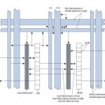
In the above diagram the buffering and drive stage has an inverter with a single PMOS device used as a half-latch to restore high levels after the single NMOS pass transistors. The final inverter size is tuned based upon the routing wire length. The NMOS pass transistors at nodes “m” and “n” represent the programmability in the routing region.Related: Five Things You Don’t Know About MunEDA…and One You Do

The performance and optimization goals were to:

[LIST=1]

  • Achieve 5% faster delay time
  • Match the delay between rise-rise and fall-fall times on the routing drivers within 2ps
  • Reduce the layout area by 5 to 10%

    The basic flow for transistor-level design and optimization at Altera is shown below:

    Schematic capture is done with the popular Cadence Virtuosotool and then circuit simulation can be done with a selection of SPICE, Analog FastSPICE or FastSPICE tools. The transistor optimization step is done with a tool called WiCkeDfrom MunEDA.

    An initial circuit simulation was run to establish a base line on three different driver circuits, where only DriverA actually met the driver delay goal of < 2ps:

    The WiCkeD simulation analysis included:

    • Simulation
    • Deterministic Nominal Optimization
    • Worst-case operation

    Driver A was run through optimization and showed an area reduction of 12% (Green is in spec, Red is out of spec). Charts on the left-hand side are for the delay times of fall-fall, and rise-rise, respectively. The upper right chart is the delta in time delay between rise and fall. Area reduction is the final chart in the bottom right:

    Results for Driver B after optimization show an area reduction of 9%:

    Finally, results for Driver C after optimization show a 15% reduction in area:

    In the GUI for WiCkeD you can see a comparison of nominal versus worst-case values after optimization:

    Summary

    Three different driver circuits were simulated and optimized at the transistor level using the WiCkeD tool to:

    • Achieve a balance in rise and fall times
    • Reach area reduction goals
    • Run simulation and optimization in a reasonable amount of time
    • The delay times were a bit off from design targets, but still within an acceptable range

    Read the complete 32 page presentation here.

    Upcoming Events

    You can visit with MunEDA at the following events in September:


  • FinFET Design for Power, Noise and Reliability

    FinFET Design for Power, Noise and Reliability
    by Daniel Payne on 08-29-2014 at 4:00 pm

    IC designers have been running analysis tools for power, noise and reliability for many years now, so what is new when you start using FinFET transistors instead of planar transistors? Calvin Chow from ANSYS (Apache Design) presented on this topic earlier in the summer through a 33 minutewebinar that has been archived. There is a brief registration required to view the archived webinar.

    Related: FinFET Based Designs Made Easy & Reliable

    A quick recap of why FinFET device characteristics at 14nm are better than bulk at 20nm or 28nm include:

    • Improved speed
    • Reduced power
    • Higher device density

    This chart shows performance versus VDD values for three technology nodes: FinFET at 14nm, 20nm planar and 28nm planar:

    As the value of VDD lowers, the circuit delay improvement of the FinFET increases versus planar devices. On the downside, FinFET designs add new challenges like:

    • Reduced noise margins
    • Reduced EM (Electro Migration), ESD (Electro Static Discharge) tolerance
    • Increased temperature effects
    • Higher device capacity

    The specific EDA tool that ANSYS offers for power, noise and reliability analysis is called RedHawk 2014 and it addresses each of the new challenges:

    Instead of analyzing chip and package separately for IR drop, the recommended approach is a simultaneous analysis using a distributed model of the package instead of a simple, lumped model. Shown below are IR drop analysis results of chip and package, first using a lumped package model which has a 13.8mV drop, next using a distributed package model which shows a more accurate 19.2mV drop value:

    Typical runtime to do a package extraction with RedHawk-CPA on a 6 layer package is 10 minutes, while using about 15 GB of RAM. To do the IR drop simulation required just 58 minutes and under 8 GB of RAM.

    FinFET Foundries
    The FinFET processes at TSMC 16nm v1.0 and the Intel custom foundry at 14nm are certified for use with RedHawk 2014 on the following types of analysis:

    • Resistance correlation
    • EM rule handling
    • IR, Dynamic Voltage Drop extraction and analysis

    I would expect support for FinFET processes at Samsung and GLOBALFOUNDRIES in the near future.Related: Intel & ANSYS Enable 14nm Chip Production

    Analysis
    With higher drive currents, it’s even more important for FinFET designs to have layout checks for connectivity analysis like:

    • Missing vias
    • Power and ground grid weakness check
    • Resistance checks
    • Power/Ground balance
    • Switch placement
    • Pad placement
    • IR drop checks
    • High power density checks

    Reliability analysis includes things like: Electro Migration (EM), thermal and Electro Static Discharge (ESD). Power noise analysis looks for issues of: dynamic voltage drop (DVD) on the power grid, low power compliance with multiple voltage domains, and the impact from power noise on timing. As an example, here’s a plot showing analysis results for timing hotspot and a DVD map, so you can focus first on fixing the IR drop issues in the timing hotspot area:

    Summary

    The engineers at ANSYS have a long history of building EDA tools for power, noise and reliability analysis. Now they’ve extended that experience into newer IC designs using FinFET technology from foundries like TSMC and Intel using the RedHawk 2014 software release.


    Improving Complex System Design

    Improving Complex System Design
    by Paul McLellan on 08-29-2014 at 7:01 am

    Next week Mike Jensen of Mentor will present a webinar Improving Complex System Design Reliability and Robustness. The webinar will be presented live twice and presumably available for replay soon after, as is usually the case:

    • September 4th 6.00-6.45am pacific (9pm in Asia, 3pm in most of Europe)
    • September 4th 10.00-10.45am pacific


    This is actually a webinar about Mentor’s SystemVision multi-physics development environment. The webinar will cover how using model-based design can produce order-of-magnitude improvements in productivity and quality and help ensure the reliability and robustness of your next system design.

    Complex systems require a unique design approach to ensure reliable and robust performance. A model-based design methodology provides a virtual system incubator for evaluating design ideas, analyzing parameter variability, optimizing costs, and jump-starting production. Using this approach, advanced individual component models overcome limitations in traditional approaches and account for manufacturing and environmental variations so that the integrated system model reflects the cumulative variability. Tolerance stack-ups can be evaluated, and reasonable performance margins verified, resulting in improved design reliability, and lower system and warranty costs.


    Mike will showcase robust design methodologies for system development, focusing on statistical and parametric analysis methods (Monte Carlo, sensitivity, worst case) presented in SystemVision. SystemVision supports full-featured model development using both VHDL-AMS and SPICE formats, simulates systems at multiple levels of model abstraction, quantifies the effect of variation in component performance, and is fully integrated with the popular DxDesigner / Xpedition environment from Mentor Graphics.

    This is a product which spans a huge range of capabilities and has a correspondingly broad range of people who would benefit from attending: system engineers, control engineers, mechanical engineers, engineers developing test environments for complex multi-domain systems, engineers doing analog, digital or mixed signal design. And of course, people managing groups in these areas.

    More information, including a link to register for the webinar, are here. More information on SystemVision is here.


    Also, if you are in automotive in Michigan, there is a special automotive U2U meeting in two weeks on September 10th in the Aurora Hotel in Dearborn. Details, including a registration link (it’s free) are here.


    More articles by Paul McLellan…


    New details on Altera network-on-FPGA

    New details on Altera network-on-FPGA
    by Don Dingee on 08-28-2014 at 4:00 pm

    Advantages to using NoCs in SoC design are well documented: reduced routing congestion, better performance than crossbars, improved optimization and reuse of IP, strategies for system power management, and so on. What happens when NoCs move into FPGAs, or more accurately the SoC variant combining ARM cores with programmable logic?

    One of our own SemiWiki readers left this comment in a discussion on one of these SoC architectures a while back:

    What would be interesting is some NoC tools that can abstract the buses away so that you are not stuck with a particular AMBA/AXI implementation and can use the FPGA fabric for communication transparently without knowing what buses are being used.

    The academic community has also been contemplating the benefits for a while. Mohamed Abdelfattah gave an interesting talk in a University of Toronto seminar a couple years ago – his introduction lays out the benefits of NoCs over unstructured FPGA interconnects, and he raises a scenario of an FPGA-tuned hybrid hard/soft NoC and its advantages.

    Point of that discussion: don’t just grab NoC IP and take the DIY route to lay it on top of an FPGA design. What is needed is a much more integrated approach, which delivers benefits with efficiency. Last year, Arteris announced that Altera licensed FlexNoC, and a lot of folks were wondering what that would look like. The press release gave some non-specifics about timing margin and frequency requirements, and we’ve been waiting for more to be revealed.

    There may have been documentation floating around under NDA, but a few days ago Altera publicly updated the user manuals for the Arria 10 MPSoC as they ramp up from sampling (now) to general availability (soon). I’m not here to debate “industry’s only 20nm”, or the DSP capability, or the competitive timing – we’ll leave that for some other day. I want to focus on the difference the Arteris NoC makes when tightly integrated into an FPGA.

    The new document of interest is the Arria 10 Hard Processor System TRM Chapter 7, System Interconnect. A big point of interest is the seven independent level 4 buses, each on its own clock domain. This allows data traffic to flow at multiple performance levels. To our reader comment from earlier, the L4 buses also support multiple protocols: AMBA AXI, AHB and AHB-Lite, APB, and Open Core Protocol (OCP).

    Security is also right at the top. Using the firewall capability of the NoC, users can configure access privileges on a per-peripheral and in many cases a per-transaction basis. There are actually two layers of firewall on the SDRAM, one working with the accelerator coherency port of the ARM core, and a second used when cache misses occur. This could be a significant architectural plus in not only secure communications, but safety partitioned designs.

    It is fast; one sentence says it all:

    The main portion of the system interconnect runs at up to half the MPU main clock frequency (mpu_clk).

    That would translate to 600 MHz, combined with an 800 MHz FPGA fabric clock. The NoC is not adding a lot of unwieldy overhead getting in the way of performance. There is also the aspect of NoC software abstraction to consider. It would be extremely difficult, not to mention slow and bloated, to recreate what Altera has done integrating the Arteris FlexNoC in this device.

    In closing, I’d emphasize while the view from 50,000ft is similar – a dual ARM Cortex-A9 in an FPGA – the details of the Arria 10 MPSoC are quite different from that other device we talk about a lot. It’s hard to say a feature makes something clearly better or worse in the overall context; it really depends on what an application is trying to do that makes one architecture more suitable than the other. This network-on-FPGA approach may open some new doors, particularly in terms of the firewall capability, that were previously hard to implement.


    Related articles:

    Compositions allow NoCs to connect easier

    A song of optimization and reuse


    Granite River Labs and TSMC Expand Agreement

    Granite River Labs and TSMC Expand Agreement
    by Paul McLellan on 08-28-2014 at 7:01 am

    For several years now, TSMC has run increasingly sophisticated IP validation. Ramping a new process as a foundry requires a number of things to all come together almost simultaneously: the process, of course, and some designs to run and start to recover the huge capital investment a modern fab entails. With many SoCs having over a hundred IP blocks, getting the IP qualified is an essential part of a design team being able to get a design into production. Taking a systematic approach to IP quality is paramount for successful SoC products.


    TSMC’s latest IP validation has multiple steps, increasingly expensive to execute but with increasing confidence level in the IP. The first 3 steps are a review of the IP without manufacturing it. The later steps involve running extensive tests on IP that has been manufactured, typically in a shuttle run for a new process that is not yet in volume production. For more mature processes where a lot of IP has been in use for many years, the sheer number of designs in successful volume production is its own guarantee of IP quality.

    [LIST=1]

  • Physical review (DRC, LVS, ERC, antenna checks)
  • DFM compliance (DFM-LPE, LPC, dummy fill, VCMP)
  • Pre-silicon assessment (design kit review, design review)
  • Silicon assesment (tapeout review, silicon report review)
  • Split lot silicon assessment (split lot tapeout and report review)
  • IP Validation Center (audit IP testing results by TSMC test lab)
  • Volume production

    Last month, TSMC’s IP Validation Center and Granite River Labs deepened their relationship and further expanded the TSMC9000 IP validation ecosystem. This covers expanded test capacity, test auditing and posting IP validation results on TSMC-online. This is a part of item #6 above, leveraging the expertise of GRL in the test and validation of high speed interfaces.

    GRL will serve as an IP validation partner to TSMC. The test methodology development and correlation will be done at GRL’s office in Hsinchu (where TSMC is headquartered of course). The bulk of the work will be carried out at GRL in Santa Clara and Bangalore. TSMC will subcontract to GRL to create a test methodology for the specific PHY. GRL can then use their extensive expertise and wide range of costly equipment to perform the testing. The results will then be available through TSMC-online like where it can be searched by potential users.


    GRL has extensive electrical test facilities using Introspect, Teledyne Lecroy, Tektronix, Keysight and others. They also hav protocol test solutions that can handle error injection, stress testing, protocol exerciser automation and so on. They have R&D sites in Oregon and Japan. Labs in Santa Clara, Bangalore, Penang, Hsinchu and Taipei. The Asian HQ is in Singapore, worldwide HQ is in Silicon Valley.


    More articles by Paul McLellan…


  • Xilinx UltraScale gives you 25% more packing than you know who…

    Xilinx UltraScale gives you 25% more packing than you know who…
    by Luke Miller on 08-27-2014 at 11:30 pm

    Coke with no ice. You see I am not cheap, or even frugal but a good steward. One of the things that I hate the most is waste. You know lights on in every room, door open during winter and driving 25 miles to save a dollar on gas.

    One will notice fairly quickly that with Xilinx UltraScale 20nm FPGAs coupled with the new-fangled analytical router that the Xilinx UltraScale FPGAs are very lean on waste. There is nothing more frustrating than to plan your FPGA design and only hit 50-60% full before one has timing and/or routing issues. Xilinx has a very good white paper just out that I would encourage you to read. It is wp455, ‘UltraScale Architecture: Highest Device Utilization, Performance, and Scalability’.

    I will quickly note here, the paper mentions the ‘competition’. Now, I do not want to be presumptuous here, nor name names, so I will not mention that the competitor is Altera, which would not be prudent, after all it could be Achronix, right? But certainly not Altera. Shucks, who am I fooling, it is Altera.

    A nice test case was run, both the Arria 10 (I assume) and UltraScale 20nm. Both used the SAME design code, from Open Cores and off you go. The results, as expected hammered the competition. See Below:

    Before you get all spun up here, BOTH devices had about the same logic cell density of about 1160K cells. This is a blind test, all things equal. No griping please. UltraScale roughly was able to use 25% more resources than Altera. This a real deal, and a big deal. Do you like paying for resource you cannot use? No one does! The test also highlights the differences not only in Xilinx’s ability to route better but the architectural improvements that are superior to Altera. Xilinx rebuilt its router and pretty much their FPGAs.

    The other highlight of the white paper comes in the form of scaling using Xilinx UltraScale. This means design migration from 20nm to 16nm. “For example, any UltraScale FPGA in a package ending D1924 is compatible with all other UltraScale FPGAs in D1924 packages. This strategy provides package footprint migration between Kintex UltraScale FPGAs and Virtex UltraScale FPGAs built on both 20 nm and 16 nm FinFET processes.” This is great as PBC rework is both costly and time consuming.

    Rounding out this white paper 455, is the fact that Xilinx’s UltraScale has ASIC like clocking. This is key, not only in timing closure but the ability to pack fuller, tighter designs at a higher clock frequency. So you can use more of the Xilinx FPGA, and more cycles in the Xilinx FPGA. That is a double whammy. Speaking of which, remember that show with the whammies? Big bucks, no whammies stop… I will leave this blog on a very corny note; if you want no whammies in your design, then may I encourage you to read up on Xilinx, and make the wise choice for your next design, or even your current design, it may not be too late to switch, you truly will not regret it.

    Also read:

    Develop High Performance Machine Vision in the Blink of an Eye


    Silicon Measurement Data Gives Insights to Using Metal Fill With Inductors

    Silicon Measurement Data Gives Insights to Using Metal Fill With Inductors
    by Tom Simon on 08-27-2014 at 4:00 pm

    Metal fill requirements for inductors are now a fact of life. Fill has long been seen as detrimental to device performance due to parasitic capacitance. The necessity of fill arises from the need to ensure planarization of dielectric layers by using chemical mechanical polishing. Without adequate fill, areas of the chip can suffer from uneven planarization.

    If using fill is inevitable the first question to arise is how can designers minimize its impact? The design community has had to rely on intuitive answers as to what the impact actually is and consequently how to reduce it. It is axiomatic that regardless of the level of impact, if it can be accurately modeled, then successful designs incorporating fill can be built. In the absence of a quantitative way to assess the impact of fill, designers are working in the dark, and assuming unwanted risk.

    3D Electromagnetic solvers simply are not up to rigorously solving for the hundreds of thousands of elements that are seen in filled inductor layouts. So naturally designers sought to eliminate fill from their designs. If fill is not present in the design then there is no need to accurately model it.

    Nevertheless Lorentz Solution has run PeakView to rigorously solve test cases of limited size to learn more about metal fill impacts on inductor performance. A variety of fill shapes and structures were used. Even eddy currents inside of fill elements was looked at. One of the first things learned was that adding stacked vias to metal fill creates large capacitive coupling to the substrate. This is intuitive, as the ‘plate’ is effectively moved to the bottom metal, much closer to the substrate.

    It is easy to comply with foundry rules for via fill without placing connecting vias in all the metal fill structures. Typically via fill density requirements are on the order of single digit percentages. So moving forward it was decided to focus exclusively on floating fill without inter-layer connections.

    At low fill densities there is a minimal bottom place capacitance shift when the fill is fully floating. To come up with data concerning higher densities and with fill on all layers, as would be seen in production silicon, Lorentz concluded that the only reliable way to proceed is with silicon data.

    Lorentzteamed up with Altera, TSMC and Mentor Graphics. Lorentz Solution designed inductors at 20nm and embedded them in test keys. A series of different fill shapes and densities were applied to the device under test. The silicon was fabricated and measured by TSMC, who generously agreed to assist in this effort. As the next step, Lorentz de-embedded the raw data and performed data analysis.


    What made this project useful is that PeakView has a method for simulating metal fill that dramatically reduces the size of the problem. This feature is in PeakView’s CMP package. The CMP package, in addition to handling fill intelligently, automatically merges slotting and striping commonly found in wide metals. PeakView’s CMP Package can automatically identify metal fill in designs. This alleviates the need for a manual step prior to EM simulation to remove fill from the layout. Once the fill is identified, the user can choose to have the simulation ignore it, or have it modeled.

    Silicon test chip data was used to show a good match with PeakView CMP results. The other valuable thing learned was that the fill densities and structures used had negligible impact on L and a very small impact on Q – and that was mostly from a slight addition to the parasitic capacitance.


    With hard data showing that fill can have a low impact and that this impact can be properly modeled, designers should be much more comfortable using recommended fill densities in their designs. Now let’s analyze the potential benefits of using recommended fill.

    When metal fill is used, the result is a more planar assembly of the dielectric and metal layers. The foundries provide detailed information on the process geometry in technology files that are used directly or indirectly in every aspect of the design flow. TSMC provides iRCX files and other foundries use ITF files for this purpose. Every tool that relies on this information relies on the fab producing silicon that conforms to the foundry specification. Simply put, using fill that is out of range can produce silicon stack up geometry that does not match the iRCX or ITF data provided. This exposes designers to an unforeseen risk because analysis tools may be working with input files that do not reflect what was fabricated.

    It is well understood that without metal fill, inductors may be the source of moisture infiltration into the die. After moisture enters the chip, it can rapidly move to device junctions, causing catastrophic chip failure. Some foundries insist that seal rings be used when fill is reduced to avoid issues arising from dielectric damage.

    Seal rings also take up room on the die, and do not always provide a significant beneficial design effect other than creating a moisture barrier. What if designers could remove seal rings? Suddenly it is looking like with the combination of stack up information integrity and area savings that fill might not be so undesirable.

    In conclusion silicon data shows that when fill is properly designed its detrimental effect is not significant. Further, the extent of this effect can be simulated effectively by PeakView’s CMP Package. Lastly there appear to be good reasons to maintain the fill densities that are recommended around and underneath inductors.

    The value of a thorough study of the effects of fill at 20nm has been shown useful in removing confusion regarding the role of fill in inductors at advanced process nodes.


    Broadcom Internet of Things

    Broadcom Internet of Things
    by Paul McLellan on 08-27-2014 at 7:01 am

    One of the perks of blogging here is being able to get a press invitation to lots of events, often in interesting locations I never even knew existed. Tonight it was a Broadcom event in SPUR here in San Francisco. The evening was about the Internet of Things (IoT). Everyone knows that IoT is sort of hype, but it is also a real opportunity. Not that there is just one market some big guy can dominate, but it is lots of little markets for stuff you would never think of.

    So here are a few of the “things” I saw this evening:

    • a wireless toothbrush. whenever you use it it uploads data on how long you brushed and where to the cloud. so you can track how conscientious you are. Or more likely, your kids are
    • a big red flashing light with a Bud logo on it, sold in Canada. You set it up with your favorite hockey team (Sharks round here!) and when a game is about to start or when the team scores the light flashes and it shouts for the team. I think it suggests you have a Bud too. They produced a few as a small project, they sold out instantly and since then they have made lots
    • a little toy for kids that records voicemail and when they reply it feeds it back to your mobile phone

    Broadcom was actually talking about a platform called Wiced. It is a prototyping kit for people wanting to build IoT projects. It has multiple sensors (temperature, humidity, gyroscopes etc) and Bluetooth connectivity. So you can be up and running in literally minutes. Although Broadcom are a chip company, of course, it comes with a full software stack and support for iOS and Android Apps, big data stuff in the cloud and so on. They announced the product just recently and already there are companies with Apps and more.

    A lot of the key IoS things are built-in: tamperproof encryption, authentication and privacy controls. In some IoS areas such as games we don’t care that much about this stuff. But other areas, such as medical devices or our cars then we care a lot. These are life critical areas, to say the least.


    One thing that makes IoT so interesting is that there are no large dominant companies. It is an open field. Lots of devices and ideas, thousands of players, no monopolies, and a low barrier to entry for startups. Some parts of the business will end up being SoCs I’m sure, but for now most of it is integrating microcontrollers, sensors and more. Get the Broadcom chip and add software, for example. If it is a big success you can cost reduce it later. But for now it is all about getting stuff to market and seeing what people are interested in. As the old saying goes, throw it against the wall and see what sticks.


    More articles by Paul McLellan…


    Do you check your circuit DC stability?

    Do you check your circuit DC stability?
    by Jean-Francois Debroux on 08-26-2014 at 8:00 pm

    Most analog designers are aware of loops stability. In most cases, stability is understood as AC stability, the goal is ensuring enough phase (gain) margin so as to avoid the loop to enter oscillation. But prior to studying AC stability, DC stability should be questioned. What is that DC stability only few people think of?
    Continue reading “Do you check your circuit DC stability?”


    Opting for ARM software scalability

    Opting for ARM software scalability
    by Don Dingee on 08-26-2014 at 12:00 pm

    Behind much of the success of ARM architecture is a scalable software model, where in theory the same code runs on the smallest member of the family to the largest. In practice, there are profiles, and a variety of hardware execution units, and resource constraints in low power scenarios that enter the picture. As a result, operating systems have evolved very differently.

    Going “bare metal” or with a very compact kernel solves some of the problem at the low end; developers can work close to the hardware and #ifdef around support for variations in resources. If one needs more advanced features, such as graphics, connectivity stacks, and virtualization, or is hoping to build on value from somewhere in the open source community, an operating system with a defined set of APIs becomes much more important.

    Coming from the other direction, full featured operating systems haven’t scaled down well to microcontrollers, with the biggest roadblock partitioned memory requiring an MMU implementation. The ability to virtualize memory and harden against task crashes is a huge plus, as the popularity of Linux and Android attest. With improvements in processor speed, the term “real-time” on larger cores has become more of an issue of controlling background tasks instead of interrupt response and context switching times.

    Scanning the commercial and open systems offerings for operating systems usually provides a very different answer in support for ARM Cortex-M versus ARM Cortex-A, even leaving out the latest 64-bit ARMv8 discussion. There are, of course, a handful of operating systems that straddle the boundary, generally in the vein of microkernels scaling up.

    One of the optional hardware execution units in the Cortex-M architecture is a memory protection unit (MPU), available on Cortex-M4, Cortex-M3, and Cortex-M0+ cores. It provides eight protection regions, which can implement the basics of access rules and task protection running out of flash without creating a full-blown virtual memory model and the complexity of MMU programming.

    Mentor Graphics has just extended their Nucleus RTOS into this space, offering the same reliability from their experience with industrial and medical applications in MCU territory. By leveraging the MPU, they are bringing the same process model across the ARM spectrum. Developers still have access to the more advanced features of Nucleus on bigger ARM cores, including a multicore framework for mixing and matching operating systems.

    The key observation here is in smaller devices, applications often don’t need a huge number of tasks and memory partitions – but having just a few may make a difference between either risking integrity of an application, or having to go up to a much bigger and hungrier SoC. MCU vendors are generally seeing the light, offering the optional MPU on Cortex-M as standard fare, and enabling a lightweight version of the same techniques previously only on larger Cortex-A cores. It is another example of how MCU and SoC space is starting to blur.

    Hardware and software teams need to carefully think through use cases when deciding what to include and what to omit. There may be short term savings in opting out of some execution units when tailoring an ARM implementation, but in the long term those features may emerge as very valuable. We will likely see more of these fine-grain decisions – memory protection, encryption, and DSP extensions among the candidates for support – favoring inclusion moving forward, helping software scale better across ARM processor families.

    Related articles:

    The Secret Essence of an IoT Design

    More “toddlers” innovating on the IoT