Yesterday, Silvaco announced that it has acquired Invarian Inc. Details of the transaction were not disclosed.
Who is Invarian? They are a recognized leader in block-level to full-chip sign-off analysis for complex, high-performance ICs. Their unique methodology utilizes a parallel architecture and concurrent power-voltage-thermal analysis to provide engineers with fast, accurate, and consistent results from the gate level through the 3D package environment.
Invarian has several products, all under the InVar umbrella name:
- InVar Pioneer Power, power analysis platform for custom and standard cell based designs
- InVar Pioneer IM/ER, full visibility of supply networks from top-level connectors down to each transistor
- InVar Pioneer Thermal, the industry’s largest capacity and most accurate thermal sign-off analysis
- InVar Pioneer Macro Modeling, hierarchical modeling to enable fast full-chip analysis while maintaining true to life accuracy from IP and blocks to top-level design
- InVar Frontier 3D Thermal, static and transient thermal simulator based on the variable splitting method for efficient prediction of temperature distribution for 3D ICs
Having great technology is a good start but on its own it is not enough, foundry support is also important, and given its gorilla status nowhere is as important as TSMC. The InVar product family is TSMC certified for 20nm and 16FF+ v0.9 to enable sign-off analysis accuracy for static & dynamic IR drop analysis and EM verification, and the collaboration is on-going to conclude 16FF+ v1.0 certification.
My old Cadence colleague Suk Lee, now TSMC’s Senior Director of Design Infrastructure Marketing said:TSMC and Invarian have collaborated to ensure that customers have confidence when they perform EM or IR-drop analysis. We look forward to continuing this collaboration with Silvaco with our advanced process nodes.
Today I met with Dave Dutton, Silvaco’s CEO. One piece of trivia I learned is that the Silvaco name was never intended to be the permanent name of the company, it just stands for “silicon valley company” and is not some clever acronym involving simulation, layout and verification. But company names are not always very deep: Apple was supposedly so-named primarily to be alphabetically ahead of Atari.
Another thing he told me is that after several years of absence Silvaco is going to be back at DAC with a 600 square foot booth (#532 for those of you making really early plans). It is no secret that Silvaco’s founder Ivan Pesic, before his unfortunate death, was not really a believer in marketing (except billboards) and as a result Silvaco’s visibility in the industry is a lot less than it should be for a company of their size. Some people are surprised to discover that they even still exist, let alone that there are market segments in which they are the leader. Amit Nanda, the VP marketing, joined us in the meeting: it is his job to change that perception.
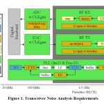
There is already some level of interoperability. For example, the above diagram shows co-simulation using Silvaco’s SmartSpice with Invar Electrothermal co-simulation.
The Silvaco press release is here. The Silvaco page on InVar is here.