webinar IPXACT banner

Apple’s ARMed History

Apple’s ARMed History
by Majeed Ahmad on 03-24-2015 at 7:00 pm

Apple has redefined three industries within a decade: media player with the iPod, mobile handset with the iPhone and portable computers with the iPad. If there is anything common in these three game-changing product development stories other than Apple, it’s the ARM footprint. Even now the technology media is abuzz with speculation that Apple could eventually replace Intel’s x86 chips in Macs with ARM SoCs.

In retrospect, Apple’s association with ARM goes far beyond the iPod/iPhone/iPad success stories, right up to the foundation of the British technology icon. In many ways, it was Apple who had put ARM on the semiconductor industry map. It’s a fascinating tale of technology collaboration that was born out of specific design needs of the Cupertino, California–based computer firm.


Search for a specialized processor for Newton led to the creation of ARM

During the late 1980s, Apple was looking for a suitable mobile processor for its upcoming PDA that came to be known to the world as Newton. Here, Apple’s fab partner VLSI Technology led the computer maker to a small firm in Cambridge, England that owned a low-power and high-efficiency processor. Acorn Computers, also a PC maker, had developed its own processor because it didn’t want to buy expensive PC processors from Intel or Motorola.

However, Acorn didn’t have deep pockets to develop a complex and powerful processor, so it ended up with a RISC-based device carrying a simple structure. They called it Acorn RISC Machine or ARM. In VLSI, which manufactured these PC processors for Acorn, it was John Stockton who had told the Newton team about the ARM processor. Eventually, Apple’s chief scientist Larry Tessler made the case for using ARM processors in the Newton PDA.


John Stockton showed the Newton design team way to ARM processors
(Photo: Mayfield)


The Birth of ARM

Now Apple wanted to make some tweaks in the original ARM processor to suit the needs of Newton and Acorn didn’t have the budget to carry out these changes on its own. In fall 1990, in a span of six weeks, a joint venture was negotiated between Apple, VLSI Technology and Acorn. Acorn would provide the manpower, Apple Computers would bring the financial support and VLSI Technology would share the design tools technology.

On November 27, 1990, Acorn joined hands with Apple and VLSI to jointly create a new company that changed its name from “Acorn RISC Machine” to “Advanced RISC Machine.” Robin Saxby officially launched Advanced RISC Machines or ARM with the goal to address and attack the growing market for low-cost, low-power, high-performance 32-bit RISC chips. Apple, who had persuaded Acorn to make the ARM platform independent, took a 43 percent stake in the new company for US$3 million.

Apple began using the first generation of mobile ARM chips in its Newton Message Pad launched the 1993. In addition to supplying chips to Apple and Acorn, ARM began licensing the rights to manufacture its chip designs as well as offering an architectural license to technology firms interested in incorporating and modifying ARM’s core technologies into their custom chip designs. ARM quickly became the de facto standard for embedded and mobile chip designs. The rest, as they say, is history.

As a small footnote, it’d be worthwhile to mention that ARM returned the favor by providing a much-needed stream of cash to Apple during its bleak days in the late 1990s. From 1998 to 2003, Apple sold its shares in ARM for an estimated US$1.1 billion, the cash infusion that helped Jobs to finance new projects and rebuild the beleaguered computer maker. In the hindsight, Apple’s investment in ARM went on to pay huge dividends as the Cupertino, California–based technology company branched out into portable devices like the iPod, the iPhone and the iPad.

Majeed Ahmad is author of books Smartphone: Mobile Revolution at the Crossroads of Communications, Computing and Consumer Electronicsand The Next Web of 50 Billion Devices: Mobile Internet’s Past, Present and Future.


This Market worth $1,465.62M by 2020!!

This Market worth $1,465.62M by 2020!!
by Eric Esteve on 03-24-2015 at 10:52 am

This is exactly what you will never see in IPnest surveys (and written in Semiwiki):“Advanced Process Control Market worth $1,465.62 Million by 2020” …sorry for you if you like very precise figure (like $ 1, 465.62 million) but you will NEVER see such insane forecast in any of our surveys or blogs. Building a forecast is a difficult exercise, essentially based on assumptions (except if you have bought a crystal ball) and we will list the reasons why it’s far to be easy- and can’t be precise at 1/100, 000.

Before even thinking about building this forecast, you need to make a market size evaluation (as precise as possible, say at less than 1 %). In certain cases, you simply can’t access to these data, but let’s imagine that you can do it. Then, you propose a snapshot of the market status as of today (in fact, last year). If you have been rigorous, this market view will be useful for the various actors, suppliers, customers or acting in support functions to this market. You can find below a good example of a well-done job: ranking of the Semiconductor Top 20 in 2014 by IC Insights:

Even if such a ranking from independent analyst is very useful, customers will more likely ask for a forecast, usually 5 years long. At this point, you are leaving the comfortable, rational area to enter into “forward looking” type of analysis. I mean that you have to think in term of assumptions, not actual data. When you are doing a serious job, such assumptions are comforted by a deep knowledge of the specific market you are reviewing. Let’s add a few insights coming from key actors and private discussions held with some people (from your network). In fact, assumptions are only to be used after making an exhaustive review of the market under review, starting from the above table if you plan to forecast the semi market for example. One option can be to segment this market into high-end, mainstream and low-end segments or into analog, memory, processor and logic segments. Splitting to better evaluate each of these segments as the market dynamics will be different from one segment to another.

At this point of time you can start using forecast maker’s best friend: Excel spreadsheet. If your assumptions are based on rational, if you don’t make any mistake when turning it into formulas, pushing Excel button will give you results that you may organize into nice curves or table and print. By the way, don’t forget to check if the result at 1 year makes sense (and rethink the whole process if it doesn’t, identify why and correct). Once you think your forecast is solid and you come to a result you can share with customers or partner (or with your boss), PLEASE don’t print figures with 8 digit precision! This is simply NON-scientific; anybody having passed a degree in physics should know that the final precision when giving a result is always less than the weakest part of the equation. In this case, the precision linked with your assumptions…

Every time I see such results for a 5 years forecast (1, 465.62 million), my first reaction is to think that the person who has built this forecast is just… non-scientist, and I strongly doubt about the results accuracy.

PS: in 2009 IPnest has built the first 5 years forecast for the “Interface IP Market”, see above. In 2008, this market was weighting $240 million, and the forecast for 2013 was $425 million. If I am ashamed when looking at the syntax or the way this first survey is organized, I am very proud when realizing today that the 2013 actual market result is accurate by less than 5% with the forecasted market size in 2009…

PPS: For 2020, IPnest is predicting the Interface IP market to weight $820 million (not K$ 820, 150.17)… see you in 5 years.

From Eric Esteve from IPNEST


A Brief History of Kilopass

A Brief History of Kilopass
by Paul McLellan on 03-24-2015 at 7:00 am

Kilopass was founded back in 2001 by Jack Peng, whose background was in FPGAs with his most recent position being manager of technology development at Actel (now part of Microsemi). The idea was to build a company making one-time-programmable (OTP) memories using anti-fuse technology. Fuses in home-wiring (OK, I know, we all have circuit-breakers these days) work by melting metal and thus breaking the circuit. Anti-fuses work by punching a hole in the gate-oxide using a high voltage and thus making the circuit. Anti-fuses had been around for a long time. In fact I remember in 1988 at VLSI Technology when we started building anti-fuse devices for Quicklogic. Actel also had anti-fuse FPGAs.

The problem with the old approach to anti-fuse is that the comparatively thick gate-oxide and the high voltage required for programming necessitated a non-standard process. What Dr Peng realized was that at 180nm it would be possible to build anti-fuse devices on standard CMOS logic since the gate-oxide breakdown voltage (for programming) was less than the junction breakdown. The higher voltage needed for programming could be generated entirely on-chip.

In the early days of Kilopass, one of the challenges was that customers and foundries were not completely convinced that this approach was not going to cause reliability issues. It really took about 5 years before they got strong customer traction.

The basic idea has not changed since founding, although of course the memory cells have got smaller as they have ridden the technology wave down through process nodes as you would expect. Kilopass is an IP company. They do not manufacture OTP memories but rather they license their technology to companies to incorporate OTP registers or memories onto their SoCs.

I talked to Linh Hong, who is one of the longest serving employees at Kilopass and currently VP sales. She joined as the company in 2006 as it closed its series-C funding and was starting to achieve design-ins. Eight years ago they had around 30 customers, now they have somewhere between 150 and 200.

Today Kilopass is still an IP company supplying OTP memories as both sizable memories and as small register files. It has foundry support at TSMC from 180nm with 16nm in development. SMIC from 180nm with 20nm in development. GF from 130nm down to 14nm in development. UMC from 130nm with 28nm in development. And processes from Jazz, IBM, Grace and Dongbu Hitek. Full process grid is here.


Looking on the net I came across a quote from Charles Ng, who coincidentally used to work with me me at VLSI/Compass. He was the VP sales and marketing for Kilopass in its early days. He described their business back then:Kilopass is an IP Supplier of field programmable memory. You can program the memory content. It is an IP embedded in a SoC. Non-volatile memory means that data content is kept after the power is off. Our claim to fame is that we require only standard logic CMOS process without any additional processing at all. Volatile memory requires a complicated process which is very expensive to develop and to use.

The only thing that you might add today is to emphasize that in the current security environment, anti-fuse has another great attribute. It is basically impossible to “read” the value programmed into the OTP memory even with scanning-electron-microscopes and similar tools.

But today, when venture capitalists do little but talk about “pivoting” and “getting to plan B”, it is interesting to see just how a company can successfully keep the same value proposition for over a decade and build it up into a sizable business.

There is a page on the Kilopass website that lists the company’s chronology here.


Kilopass are having an open house on Thursday April 2nd from 11.45am to 2pm (so there is such a thing as a free lunch) at their new offices at 2895 Zanker Road, San Jose. If you will be attending then RSVP here.


Semiconductors off to slow start in 2015

Semiconductors off to slow start in 2015
by Bill Jewell on 03-23-2015 at 4:30 pm

A weak first quarter outlook for the semiconductor market is indicating a slow start to 2015. Intel recently lowered the midpoint of its 1Q 2015 revenue guidance from $13.7 billion (down 7% from 4Q 2014) to $12.8 billion (down 13%). The table below shows the estimated top 25 semiconductor companies revenue change for 4Q 2014 versus 3Q14 and revenue guidance for 1Q 2015 versus 4Q 2014. Of the 23 companies providing guidance for 1Q 2015, only four (Infineon, Freescale, Analog Devices and Maxim) expect positive change from 4Q 2014. Five companies expect double digit declines (Intel, MediaTek, SanDisk, AMD and ROHM). Some of the reasons cited for the sluggish outlook are weak business PC demand (Intel), excess inventory in the channel (AMD and SanDisk), limited supply due to technology transitions (Micron), a smartphone market transition (MediaTek), and uncertainty in electronic markets and exchange rates (ROHM).

The average guidance is a 5.1% decline. The revenue-weighted average is minus 7.5%. Using the high end of each company’s revenue guidance for 1Q 2015 results in a revenue-weighted average minus 5.0%. Over the last five years, the semiconductor market 1[SUP]st[/SUP] quarter change from the prior 4[SUP]th[/SUP] quarter has ranged from a 3.7% increase to a 5.1% decline, averaging minus 1.0%. The market could potentially experience the worst 1[SUP]st[/SUP] quarter decline since minus 16% in 1Q 2009 during the last major semiconductor downturn.

The outlook for the full year 2015 is varied. Forecasts since January fall into two general ranges: 3.4% to 5.4% (Gartner, IDC, GMR Data, and WSTS) and 7.0% to 9.5% (VLSI Research, IC Insights, Future Horizons, Mike Cowan and SC-IQ). The announced forecasts for 2016 range from 3.1% (WSTS) to 7% (our Semiconductor Intelligence or SC-IQ forecast). In December 2014, our SC-IQ forecast was 11% for 2015 and 7% for 2016. We have revised downward our expected growth for 2015 to 8% based on the projected weak 1Q 2015. We are keeping the 7% forecast for 2016.


Key assumptions are supporting healthy growth in 2015 and 2016 as shown in the table below. The International Monetary Fund (IMF) projects accelerating World GDP growth in 2015 and 2016. Gartner is forecasting accelerating growth in the combination of PC and tablet units. One area of concern is slowing growth rates for mobile phones and smartphones. Gartner expects total mobile phone unit shipment growth to pick up to 3.7% in 2015 from 1.7% in 2014, but slow to 3.3% in 2016. eMarketer projects slowing growth rates in smartphone users, from 25% in 2014 to 17% in 2015 and 13% in 2014.

[TABLE]
|-
| style=”width: 191px; height: 26px” | Annual Change
| style=”width: 77px; height: 26px” | 2014
| style=”width: 77px; height: 26px” | 2015
| style=”width: 77px; height: 26px” | 2016
| style=”width: 178px; height: 26px” | Source
|-
| style=”width: 191px; height: 26px” | World GDP
| style=”width: 77px; height: 26px” | 3.3%
| style=”width: 77px; height: 26px” | 3.5%
| style=”width: 77px; height: 26px” | 3.7%
| style=”width: 178px; height: 26px” | IMF, Jan.
|-
| style=”width: 191px; height: 26px” | PC + Tablet units
| style=”width: 77px; height: 26px” | 1.8%
| style=”width: 77px; height: 26px” | 3.7%
| style=”width: 77px; height: 26px” | 6.9%
| style=”width: 178px; height: 26px” | Gartner, Jan.
|-
| style=”width: 191px; height: 26px” | Total mobile phone units
| style=”width: 77px; height: 26px” | 1.7%
| style=”width: 77px; height: 26px” | 3.7%
| style=”width: 77px; height: 26px” | 3.3%
| style=”width: 178px; height: 26px” | Gartner, Jan.
|-
| style=”width: 191px; height: 26px” | Smartphone users
| style=”width: 77px; height: 26px” | 25%
| style=”width: 77px; height: 26px” | 17%
| style=”width: 77px; height: 26px” | 13%
| style=”width: 178px; height: 26px” | eMarketer, Dec. 2014
|-

Our forecast assumes solid growth for the key drivers of the semiconductor industry over the next few years. The trend from 9.9% in 2014 to 8% in 2015 and 7% in 2016 assumes moderating growth of some key drivers such as smartphones. Barring an economic downturn, the semiconductor market should experience average growth around 6% annually through the end of the decade.


Open Source Software Platform Fuels Automotive Innovation

Open Source Software Platform Fuels Automotive Innovation
by Pawan Fangaria on 03-23-2015 at 1:00 pm

These days, most of the innovative concepts in our cars are driven by electronics; not only infotainment systems, but also instrument clusters, safety systems including ADAS (Advanced Driver Assistance Systems), information displays, night vision, airbags, backup camera, stability control, and so on. The upcoming connected automobile ecosystem will provide the ultimate in automation and connectedness; your car can have all electronic components inside it connected with each other along with your smartphone and also with the outside world including the cloud and other cars. This kind of automation in connectivity of the automotive systems is possible only through the embedded software which is sitting on top of the smart SoCs employed in the electronic hardware of your vehicle.

In the near future, the software in a high-end vehicle can measure up to a hundred million lines of code. An interoperable and connected ecosystem of such a large software base in the vehicles can be best managed through an open standard where a large contribution from the open source developers around the world can be obtained. GENIVIis a non-profit consortium of automakers who contribute in building and sharing a Linux-based, in-vehicle infotainment (IVI) platform. Today, Linux has evolved as a network OS and is the most cost effective.


[GENIVI Software Architecture]

GENIVI’s aim is form a universal standard platform for all its members by ensuring compliance of open source middleware which can be freely shared among all. The members can add their own differentiation at the application level. Fordhas released its AppLink propriety source code and platform through GENIVI Alliance that complements the open source IVI platform with a proven framework to interact with smartphone and tablet applications. A car’s software can be upgraded just like an smartphone’s to keep it up-to-date for the long lifespan of the car. Of course, there is a larger need to address some of the specific issues such as security over the Controller Area Network (CAN).

As different types of electronics, for example, entertainment and safety get added into a vehicle, the complexity of hardware, software and connectivity grows because they have different levels of functionality and criticality. A high-end car today can have up to a hundred ECUs (Electronic Control Units). The processing required to manage such a large connected system requires a full-fledged automotive operating system; Linux with numerous capabilities in its middleware is promising to provide that level of OS support.


[Mentor’s hypervisor running on top of Mentor’s XSe AXSB hardware reference design]

Combining Linux with a safety certified RTOS on a hypervisor can enable a mixed-criticality single software platform and also reduce cost through module consolidation. In the above picture, MentorEmbedded Hypervisor is hosting two operating systems; the first is Mentor’s XSe OPTstack and XSe SuperBSP used for Linux based IVI systems, and the second is Mentor’s Nucleus RTOS to support safety systems. This is a proof-of-concept for bringing together a number of operating systems on a single platform to support multiple software applications with different levels of criticalities. For security, SELinux (Security Enhanced Linux) can be used for connected vehicles. The module consolidation is also assisted by standardization brought by AUTOSAR (Automotive Open System Architecture) consortium for various automotive software architectures.

Mentor’s Linux solution also brings XSe XStrace and Sourcery Analyzer into the fold that allow developers to look deep inside complex multi-core systems, see what’s happening in real time and troubleshoot like never before.

For a vehicle’s communication to outside world, there are V2V (Vehicle-to-Vehicle) and V2I (Vehicle-to-Infrastructure) technologies. V2V allows vehicles to communicate with each other using short-range radio exchanging data such as traffic congestion, weather condition, construction zones, and so on. It uses the unlicensed 5.9 GHz band which is used for Wi-Fitoo. Consortiums like GENIVI will need to ensure that V2V and V2I are also built around universal standards that are accepted throughout the automotive industry.

By using Mentor’s XSe AXSB reference board as a hardware platform along with the corresponding XSe OPTstack and XSe SuperBSP software platform, vehicle manufactures can start early development to effectively collaborate with Tier-1 supply chain.

An overview of Mentor’s Automotive Technology Platform which is based on GENIVI compliant Linux platform can be seen here. It’s also instrumented from kernel to graphics layer to deliver high performance graphics. As a Board Member of GENIVI, Mentor brings the experience necessary for the successful adoption of open source software by automotive tier-1 suppliers and OEMs.

The Automotive Technology Platform is available on the latest reference boards from Renesas, Texas Instruments, and Freescale. Mentor has an extensive partner network of software vendors, semiconductor companies and industry associations.


Vertical NAND Flash

Vertical NAND Flash
by Paul McLellan on 03-23-2015 at 7:00 am

You may know that up until now NAND flash has been a planar technology. But just as with SoC processes where we have had to go vertical to FinFETs, NAND flash has reached the limitations of scaling in the 20nm nodes and is also going vertical. It is not just a lithography issue but there are also reliability and voltage scaling issues. The solution is to stack memory cells vertically, increasing cell density without needing additional area for the memory array. These approaches are called either 3D NAND flash or Vertical NAND flash.

Coventor have put together a solution based on Terabit Cell Array Transistor (TCAT) technology, using SEMulator3D to evaluate process variations in the NAND string formation, especially during channel etching and contact formation. This SEMulator model has been reverse engineered from publicly available information such as conference papers and published SEM images. SEMulator3D is a predictive 3D modeling platform ideal for this sort of analysis due to its predictive modeling performance and accuracy.


Each memory cell is a gate-all-around device consisting of a metal gate atop a charge-trap flash stack, surrounding the string’s polysilicon channel; a gate-last flow is used for integrating the metal gate. The gates of neighboring NAND strings are tied together to form horizontally-oriented wordlines, which can be accessed at the edge of the flash device through contacts arranged in a staircase-like structure. See the diagram above.

I talked to Sandy Wen of Coventor about the new white paper that she has written on this work. Before joining Coventor, her background was in process equipment, in particular etch, where she worked for Applied Materials and for LAM Research. She is about to start a new project since her maternity leave starts imminently.

So how do you build such a complex 3D structure? The details are all in the white paper but the 50,000′ view is in the pictures below.

Using the model it is possible to investigate stability, sensitivity, and yield issues. For example, a parallel DOE of 180 runs was executed using SEMulator3D’s Expeditor batch processing capability. Etch process parameters such as nitride taper, lateral etch bias and oxide-to-nitride selectivity were varied, and the resulting channel cross-sectional areas were measured.The resulting virtual metrology data demonstrated the narrow process window for this cyclic etch. To ensure the channel etch reaches the bottom contact, the sidewall angle for each nitride layer must be maintained at 89° or 90°, while the polymer removal must be kept high enough to enable the etch to reach the bottom. When the sidewall angle for the nitride is 88°, the channel etch does not reach the contact bottom, and it has zero channel-to-ground contact area. In contrast, increasing the lateral etch bias in the polymer removal cycle can ensure that the etch reaches the channel bottom, but it comes at the expense of dimensional expansion at the top of the plug, another unacceptable feature.


If this was a real process being designed, rather than a model that has been reverse engineered, this sort of analysis using virtual metrology would save a huge amount of wafer-processing resources and, since it doesn’t require a full cycle through the fab, is also much quicker in getting defining the boundaries for the various parameters for train-and-error processing using real silicon. This is just one of the areas investigated in the white paper.

The bottom line is that, as with all advanced processing such as FinFETs, the interactions between different modules and understanding defect evolution has become increasingly difficult. Virtual fabrication techniques allow issues to be anticipated early, reducing development time and saving silicon runs.

The white paper can be found here.


Apple’s Ax Chronicle

Apple’s Ax Chronicle
by Majeed Ahmad on 03-22-2015 at 7:00 pm

In April 2008, Apple baffled the semiconductor industry by acquiring the system-on-chip (SoC) pioneer PA Semi for US$278 million. The acquisition, took place at the height of the iPhone fever, left the technology and trade media with an endless suite of guessing games. In the end, it was just about Apple’s quest for having better chips for the mobile devices.

PA Semi co-founder, Dan Dobberpuhl, was a pioneer in microprocessor design and had contributed to the landmark T-11, Alpha and StrongARM processor developments at DEC. After leaving DEC in 1998, He had founded SiByte, which developed the first multicore SoC device and was later sold to Broadcom for US$2 billion.


Dobberpuhl’s PA Semi served as a foundation for Apple’s SoC ambitions

When Apple unveiled the iPad in January 2010, Steve Jobs specifically called A4 the best and most complicated chip that Apple had ever designed. Initially, industry observers perceived the A4 as just another SoC that hooked up various IPs available from different companies. But then in April 2010, The New York Times reported that Apple has acquired the Austin, Texas-based chipmaker Intrinsity for an undisclosed amount.

That was about the time when people in the semiconductor industry connected the dots and began to understand Jobs’s claim of Apple’s long-term processor strategy for the iPhone and iPad. The story about the making of Apple’s first in-house SoC goes back to September 2008 when Samsung inked a deal with chip design house Intrinsity to develop a FastCore version of the Cortex-A8 which they called as Hummingbird. Meanwhile, Apple was looking for a way to speed up the Cortex-A8 CPU for its upcoming iPad.

According to some industry reports, Samsung asked Intrinsity to develop a FastCore version of the Cortex-A8 for Apple’s for A4 while utilizing it for its S5PC110 and S5PV210 chips after splitting the cost. Hummingbird was a ground-up, cycle-accurate, high-performance remake of ARM’s Cortex A8 architecture to get the CPU core’s clock speed comfortably up to 1GHz. The ARM-based small chip shop from Texas had brought to Apple that PA Semi couldn’t: a CPU core.

Apple A4 SoC: In January 2010, Apple introduced the A4 chip manufactured at 45nm process; it incorporated clock speed and RAM data bus enhancements that enabled it to drive the increased resolution of iPad. The A4 chip combined a single Cortex A8 CPU core to a single-core PowerVR SGX 535 GPU and either 256MB or 512MB of RAM. Apple also put the A4 chip in iPhone 4 and Apple TV.

Apple A5 SoC: In March 2011, when Apple introduced the more powerful iPad 2 device, it was powered by the dual-core A5 chip that featured twice the CPU power and eight times the GPU performance of the A4 chip. The A5 chip married a dual-core Cortex A9 CPU with a dual-core PowerVR SGX 543MP2 GPU and 512MB of RAM. It was subsequently used in the iPhone 4S handset and the iPad with Retina Display.

The progression from A4 to A5 revealed Apple’s strategic focus on the GPU part

Apple A6 SoC: in September 2012, Apple shipped iPhone 5 with A6, a new chip featuring an entirely custom “Swift” core design and manufactured at 32nm process. The A6 SoC married two of Apple’s custom-designed Swift CPU cores to a triple-core PowerVR SGX 543MP3 GPU and 1GB of RAM, roughly doubling the performance of the A5 in every respect. The most striking feature of A6 SoC was the in-house designed CPU: Swift.

Apple A7 SoC: In September 2013, nearly three years of releasing its first custom A4 chip, Apple launched the first 64-bit ARMv8 A7 chip using an entirely new Cyclone core design and a 28nm process. Apple, now a competitive chip designer, made a shift from Swift CPU core to Cyclone CPU core, which made the A7 chip look more like a desktop processor. The Cyclone CPU architecture had made a leap forward from small core CPUs commonly used in mobile devices to large core CPU found in desktop computers.

Apple rocked the industry by moving to 64-bit roadmap for mobile SoCs

Apple A8 SoC: The semiconductor industry was still coming to terms with the wonders of 64-bit computing that Apple had showcased in the form of A7 chip when Apple took another leap of faith in the SoC religion. The Cupertino-based computing giant announced the second 64-bit chip called A8 at the launch of iPhone 6 and iPhone 6 Plus on September 9, 2014.

A prominent highlight in the launch of A8 chip was Apple’s move away from Samsung’s fab to TSMC, something widely anticipated in the industry amid Apple’s increasingly complicated relationship with Samsung. The A8 SoC was about 25 percent faster than its predecessor in CPU tasks and 50 percent faster on the GPU side of things. It was also 50 percent more power efficient than the A7, and despite almost doubling the transistor count, the die size was nearly 13 percent smaller.

Majeed Ahmad is author of books Smartphone: Mobile Revolution at the Crossroads of Communications, Computing and Consumer Electronicsand The Next Web of 50 Billion Devices: Mobile Internet’s Past, Present and Future.


Intel and the Intel-of-Things

Intel and the Intel-of-Things
by Tom Simon on 03-22-2015 at 1:00 pm

When I joined Calma in 1982, Intel was a small company making microprocessor chips in a crowded marketplace. They had scored big with IBM who was using their 8088 in the very first personal computer. Wind River was a hatchling with David Wilner and Jerry Fiddler working out of a rented warehouse in Berkeley – I know, I hung out with them back then. And, the internet was something Universities used.

Things have come a very long way indeed. Now, of course Wind River is part of Intel, and the internet is, well, everywhere. In fact, it’s likely that you would have a panic attack if went out without your phone and had to endure an hour or two with no internet. Despite all that has changed and developed in the intervening years, there is more to come, much more.

The internet of things is upon us. Lots of companies are generating marketing buzz around the internet of things, and Intel has put out a white paper that presents a preponderance of evidence that it really should be the Intel of Things. The paper pretty exhaustively makes the argument that everything needed to construct the internet of things can be sourced from Intel.

Remember when they were a hardware company? No so anymore. In reading the paper I was struck by just how far afield they have collected offerings. For instance, while John McAfee himself is sliding into the abyss, his namesake company, now part of Intel, figures prominently in Intel’s IoT strategy, offering key security software. McAfee Embedded Control limits what code is whitelisted, ensuring no malicious code is run. The white paper mentions McAfee Endpoint Encryption as the cornerstone of data security. McAfee Integrity Control provides auditing and compliance information. Lastly, McAfee ePolicy Orchestrator provides central security management.

Intel also reviews their processor line up, for use from sensor control and fusion, to up to server class Xeon cores for building the cloud backend. One of their strong arguments is that there is a great deal of code compatibility across Quark, Atom, Core and Xeon families. And even though Wind River started out as an embedded RTOS company, they now provide OS’s for each link in the IoT chain.

Intel defines the links in the chain as “things”, gateways, network infrastructure, and the cloud. Wind River can still provide bare metal RTOS, to Linux, all the way through code stacks to implement heavy duty network layers on network and cloud hardware. In the cloud layer for application development Intel has acquired companies like Mashery and Aepona for API management and monetization. Clearly Intel wants to play in the software space.

It’s unlikely that a company developing an IoT offering will go whole hog and use everything from Intel, but it is impressive how many pieces they have put together. Even so, while they are strong in processors and networking, sensors are another key area for IoT devices. But the bigger question in my mind is how much is the internet of things like the internet itself? Or, in other words, how much of it will be developed vertically by one company, versus a mosaic (no pun intended) of contributions that add up to larger whole?

To answer this I’d like to come back to my FitBit for a thought experiment. It is a device (aka thing), and it talks to the Fitbit mothership, but how much of all the stuff in the middle does FitBit care about? Well, rightfully, it is agnostic as to what kind of phone I have, or even what kind of Bluetooth chip that is inside my phone. Also does my Fitbit care what embedded OS the network switches at Verizon’s backbone use? It’s impressive that Intel has all this capability. But will there even be one Intel customer that will get it all? Probably not. But if so, what could make it such that everything provided by Intel was used, versus the implied balkanization that the internet offers?


Wow: Synopsys v. Mentor Update!

Wow: Synopsys v. Mentor Update!
by Daniel Nenni on 03-22-2015 at 7:00 am

As a reminder, the Synopsys v. Mentor drama started when Synopsys filed a Complaint for Declaratory and Injunctive Relief on the same day (September 27, 2012) as they entered into an agreement to acquire emulation provider EVE (ZeBu emulator systems), which competes with Mentor’s Veloce family of emulators. Apparently, upon hearing about the EVE acquisition, Wally warned Aart about the alleged patent infringements by EVE and Aart’s response was swift legal action. This is the standard Synopsys legal strategy of “the best defense is a good offense”. Aart must be a fan of famed boxer Jack Dempsey. A better strategy would have been to mediate or settle since, with the recent ruling, this could cost Synopsys in excess of $100M dollars when all is said and done.

Take a quick look at thePermanent Injunction ruling of March 17, 2015. The infringement part is over, EVE infringed on Mentor U.S. Patent No. 6,240,376. The question now is damages. One thing that struck me after reading this is that the judge has a much better understanding of our industry than my previous experiences. Here is a link to one of those previous experiences:

Magma Avoids Trial by Settling Contract Suit With Prolific

That one taught me that, within the fabless semiconductor ecosystem anyway, it really was all about who had the better/most expensive lawyers since technology was baffling and using a fire hose of technical jargon was the underlying strategy for getting the most billable hours. Now the judges are much more technology enlightened and much less tolerant of fire hoses and “baseless” legal actions. This one however is the first time I have read a ruling that accurately described the ever important concept of “design wins” in our industry, absolutely.

Now let’s talk about damages. Paul Mclellan made a comment on the most recent Mentor quarterly conference call in regards to emulators that caused a “forward outlook” concern. Emulation is more critical now than it has ever been for SoC design so what is the problem here? From the transcripts Q&A section:

Wally Rhines – CEO, We were able to grow our emulation revenue this past year, but as noted, we had contribution from a large customer, which we don’t expect to have in the coming year. But we do expect that we can probably grow emulation revenue in the year ahead, the year we’re currently engaged in, in fiscal ’16…. Because we are making up for a loss in some of the momentum, we still believe that we will have overall growth but we’ll be swimming uphill in that respect…

If you look back at the ruling it specifically mentions Intel so let’s assume Intel is the large customer Wally mentioned. Intel is the industry’s largest emulation customer and coincidentally a big customer of EVE. The previous award of $36M was based on a 5% royalty fee on past sales. Moving forward the royalty will be tripled to 15% based on the fact that Synopsys knew of the patent infringement and continued sales . And don’t forget about legal and other expenses.

Let’s face it, Wally is a very clever man and he knows how Aart does business. He spoke with Aart prior to the EVE acquisition for a reason, he made the above comment for a reason, and getting Synopsys to file first was pure genius. It all goes to damages and they are going to be big, just my opinion of course.


SoCs in New Context Look beyond PPA

SoCs in New Context Look beyond PPA
by Pawan Fangaria on 03-21-2015 at 7:00 am

If we look back in the last century, performance and area were two main criteria for semiconductor chip design. All design tools and flows were concentrated towards optimizing those two aspects. As a result, density of chips started increasing and power became a critical factor. Now, Power, Performance and Area (PPA) are looked together as the prime criteria for SoCs. Since the beginning of this century the semiconductor industry (including technology, design and software) worked tremendously to optimize PPA for semiconductor chips; the latest technologies being FinFET and FD-SOI.

Today, we have started seeing temperature as a key criterion for consideration in the semiconductor design. Like PPA, temperature acts as a basic criterion at the device and chip levels. We are seeing state-of-the-art tools in the market for thermal analysis of chips and packages. Temperature is a key criterion for hand-held mobile, automotive, and storage devices and therefore for SoCs in that space.

While PPA and temperature (PPAT) definitely need to be looked at as the base criteria, my emphasis in this article is to look at the SoCs in a new context today where there are other major factors which can dominate over these basic criteria; in fact some of the other major factors effectively drive the PPAT for SoCs. There is already lot of work done for PPA and is on the table to be exploited and used in the larger context of SoCs. So, let’s look at the major factors which drive modern SoC design.

Target Segment: The days when one particular processor like IntelPentium used to address most of the computing market needs around the world are no more. Today, we have multiple segments within one market. For example, within computing or processing space, we have desktops, laptops, tablets, smartphones, and so on. Each of these addresses a particular segment in the computing space and can have varying needs. A desktop processor can be less power efficient than a tablet or smartphone processor. Similarly, an SoC for automotive application can be less area efficient than an SoC for smartphone. Again, even for a particular segment it’s not one market across the geography, the markets are further segmented across the geographical regions. A live example is about smartphone markets in USA, China, India, and so on; they are different. Hence, an SoCs should to be planned according to its target segments for what is needed in that segment, and more importantly for how long that design can survive in that market. Otherwise, you may provide the best PPA, but it can still fail in a particular market. Again, power and performance have to balance against each other; today there is no more leeway to gain on both fronts without cost and other implications.

Cost: Today, cost no longer rules the market. The market drives the cost. At the same time, wafer cost at lower nodes is increasing to an extent that the cost per transistor may not reduce substantially with further technology scaling. So, the SoCs need to be architected with appropriate functionality according to the market need and the cost which it can absorb. It’s extremely important to plan the BOM (Bill of Material) upfront according to the cost and profitability. An SoC with similar functionality can have variants with different fabrics and PPAs for different markets according to their cost structures. A recent example is about Qualcommlaunching its mid-range lines of 4G baseband processors, Snapdragon 618, 620, 415 and 425, specifically to compete in China market where MediaTekis aggressively gaining in 4G LTE chipset market with its low priced chipsets. Also, Intel is eyeing emerging markets with its low-end SoFIA processors. The upcoming IoT market will further establish ‘cost’ as a major factor for SoCs, because ‘low-cost and high-volume’ will be the key characteristic of various segments in the IoT market.

A more important observation related to cost, as I see it from business angle, is that the companies (or divisions in large companies) need to be swift in aligning their product line, R&D, procurement, and manufacturing processes according to the market segment they serve; otherwise they can never meet the cost structure of the market. It is okay for Intel to initially indulge in the so called “contra-revenue model” to gain mobile market share, but gradually, rather rapidly, it has to align the mobile product line according to the cost structure of that market.

Functionality: After firming up the top level business strategies for target segment and cost, the actual stage comes where an SoC is architected according to the requirement and driven to implementation. The functionality must come as the top consideration in implementation because that will justify the cost and target segment as explained above. One has to consider, what kind of CPU and with how many cores should be employed, is a GPU required, how much on-chip and expandable memory should be sufficient, memory controllers, interfaces, communication components, and many more. Today, there can be hundreds of functional components on an SoC and there is a lot to choose from for each component. This mandates to decide on the functionality you are going to support for a particular segment at a particular cost.

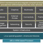
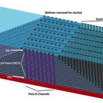
IP integration: Once the functionality is defined, not all components can be done by one company. There comes IP for various components supplied by vendors across the world. So, here the actual exercise is to choose the best PPA optimized IP for your SoC and best integration methodology for overall PPA optimization of the SoC. This optimization is at a different level where you have to architect the data traffic and communication between different components in most optimized manner to consume lowest power and have lowest latency with minimum congestion in the network. There is Network-on-Chip (NoC) available which can be utilized to manage traffic and minimize power consumption of the overall SoC. Here is an example of how Texas Instrumentsused ArterisFlexNoC in its SimpleLink Wi-Fi Family of SoCs for internet-on-a-chip solution for IoT market in home automation, safety and security, energy harvesting, industrial M2M and wireless audio streaming. This is well architected with NoC fabric to work at extremely low power. The NoC is utilized to shut down the components which are not required for a particular mode of the chip’s operation.

[Courtesy Texas Instruments: TI CC3100 Hardware Overview]

This is a very simplistic, but smart design. Imagine a design where there can be several digital and analog components and high speed interfaces that connect wires getting into and coming out of the analog IPs at different levels of voltages. The floorplanning of those IPs, IOs and busses are critical along with the software that can model the channels in the floorplan. Also, while selecting an IP, looking at its PPA in isolation is not sufficient. There can be situations where more IPs when combined together can produce innovative results. Let’s keep that aside for a more detailed article later.

System Performance: It you count on a CPU performance, it’s simply the product of IPC (instructions executed per clock) and the clock frequency. With the technology scaling, clock frequency has almost reached its limits; although with significant increase in leakage power at lower technology nodes. Also frequency itself has implications on power. The other avenues to increase CPU performance by increasing IPC include techniques such as ILP (instruction level parallelism). Several other techniques such as SIMD (Single Instruction Multiple Data) have been used to reduce the number of instructions for a task.

That was the case for a single CPU. Today, we need to look at the performance in terms of the whole system’s performance. The CPUs can have multiple cores which provide high performance with optimized power. However, to exploit the multi-core architecture, several aspects have to be considered in the SoC design. These aspects may include the number of cores ideal for an SoC requirement, special cores for graphics, speech recognition, communication protocols, cache subsystem architecture, RAM (Random Access Memory), memory access mechanisms, and so on. So, one has to consider actual definition of performance as “time taken to execute a task” and consider the complete system performance while designing an SoC. Also, considerations have to be made for how different types of software would make use of the multiple cores.

Size: The size of a chip should not be confused with the density of transistors a technology node can provide. It’s the architecture and space utilization on the chip that matters. So, it’s the absolute size of the chip which needs to be considered; can it be architected with required functionality within the parameters of the size for a particular market segment. If a robust architecture can satisfy the size with the required PPA at a higher technology node, then that’s the best scenario. One does not need to use lower node process unless essential. In cases of GPUs where there are parallel workloads, higher density of transistors (and hence lower technology nodes) can definitely improve performance almost linearly; so lower technology should be considered there. From a business perspective, size can be extremely important in wearable segment of mobile and IoT market. So, size of the actual SoC is an important criterion to consider before architecting.

I would like to take a pause here as it is getting lengthy. However, there are other important and interesting criteria to consider for SoCs (e.g. h/w, s/w, embedded and so on). I will talk about those later in part-2 of this article.