It is often said that things go in big cycles. One example of this is the design and manufacturing products. People long ago used to build their own things. Think of villagers or settlers hundreds of years ago, if they needed something they would craft it themselves. Then came the industrial revolution and two things happened. One is that if you wanted something like furniture or tools you were better off buying them. The other was there was a loss of skills; people ‘forgot’ how to make things. This meant that the ability to create was concentrated in the hands of a few, and individuals had less control over what was available to them.
The maker movement has changed all that. The ability to design and build things has come full circle. Now if you want to design with 3D Printers and Arduino boards you can design a range of things, from simple everyday items to sophisticated appliances. In many ways the Internet of Things was started through this same pathway. People took low cost development systems and tools, added sensors, wireless and often servos to make a wide variety of useful things.
Semiconductor design has followed an analogous path. Early on design teams were small and they built chips that became the components of that era’s products. I remember calling on chip design companies in the late 90’s where it was literally three guys with a Sun workstation running layout software.
That era has ended and it seems that recently the only feasible way to design chips was at places like Nvidia, Intel, Freescale, Marvell, etc. They can apply design teams with hundreds of people to build their products. If you had an idea for a design and did not have the manpower, your idea went un-built.
However, things are changing again. The same market and technology forces that drove the maker movement, and pushed for standardization of building blocks, has spilled over into the internals of chip design. With the need for increased sophistication, the tools for building integrated platforms for IoT have been growing and maturing. We all know the formula by now: MCU, on board NVM, one or more radios, ultra low power, security, interfaces to sensors and a SW development environment to build user applications.
Differentiation is the key to success; product developers know they need to optimize their platform for their specific needs. ARM recently embarked on a project to test out the real world feasibility of having a small team build a custom IoT end point device in a fleeting 3 months. ARM used the TSMC Open Innovation Platform Forum in September to present their results.
ARM Engineering Director Tim Whitfield gave a comprehensive presentation on their experience. The challenge was to go from RTL to GDS in 3 months with 3 engineers. additionally, there were hard analog RF blocks that needed to be integrated. They went with the ARM mbedOS to make it easy to prototype. They also included standard interfaces like SPI and I2C for easy integration of external sensors.
ARM used their arsenal of building blocks which includes the Cortex M3, Artisan physical IP, mbedOS, Cordio BT4.2, ancillary security hardware and some TSMC IP as well. The radio was the most interesting part of the talk. A lot of things have to be done right to put a radio on the same die as digital. The Cordio radio is partitioned into a hard macro containing all the MS and RF circuitry. In the hard IP there is also real-time embedded firmware and an integrated power management unit (PMU) – critical for effective low power operation. It comes with a Verilog loop-back model for verification. The soft IP for the radio is AMBA-3 32-bit AHB compliant. It is interrupt driven and can operate in master & slave mode with fully asynchronous transmit and receive.
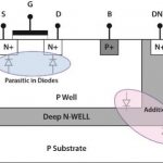
When adding the radio to the design, designers are given guidelines to avoid supply coupling in the bond wires. This is provided by adding 100pF decoupling per supply. They used CMOS process friendly MOM caps. They did receive some guidance from the radio team on how to prevent substrate coupling. They used a substrate guard ring with well-ties. Tim suggested that the guard ring could possibly be delivered as a macro in the future.
They discovered that if there was no cache that 80% of their power would be used for reading the flash and 20% used running application code. So they reduced the power overhead by using caching. Tim sees opportunity to further improve power performance with additional cache enhancements.
They already taped out in August, and are now waiting for silicon from TSMC in October. That, of course, will be the real test. Whatever lessons learned will be applied to improve the process for customers down the road.
This is certainly just a “little bit more” impressive than a maker getting their Arduino project working. Nonetheless, it is definitely a branch of the same tree. Enabling this kind of integration and customization democratizes product development and will in turn create new opportunities. I look forward to hearing how the first silicon performs.