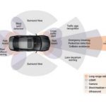
CEVA Dolphin Weninar SemiWiki 800x100 260419 (1)

Google Pixel And Home Event: A Quick, Industry Technology Analyst Take

Google Pixel And Home Event: A Quick, Industry Technology Analyst Take
by Patrick Moorhead on 11-24-2016 at 4:00 pm

I just completed watching Google’s special hardware event and wanted to share my high-level, industry analyst take on it.

Google Assistant
Everything Google showed on-stage was very compelling, but as we have seen with most claims in intelligent assistants, rarely if ever have they lived up to the hype. Until consumers can truly rely on assistants, they will continue to be a niche use case. Google Voice and Google Now are very high quality, but to claim game-changer, Google Assistant must do what it did on stage to really set it apart and I’ll have to do a lot of testing before I’m there. Consumers must keep in mind that this personal information is being mined by Google to create improved advertising profiles.


Pixel phone

Google intelligently amped up their camera development and message as consumers care about this a lot. The 89 rating on DxOMark is impressive and using a gyroscope to compensate for video jitter is unique. Now DXO mark is nice, but may not compensate for the lack of a second lens for telephoto and also, until the camera is tested, we won’t know if they’ve compromised the experience in other ways to hit that impressive score. I’m surprised Google didn’t opt for two cameras as it’s rapidly becoming standard on premium phones. Apple, Huawei, and LG have dual camera features. Free unlimited storage in highest quality mode is a great deal but only if you like the pictures. I expect Pixel photo experience to be good but probably not great by comparison.

I was really happy to see Pixel sport literally the latest and greatest Qualcomm chipset, the Snapdragon 821. Google didn’t specify support for modem features, but I am hopeful it supports T-Mobile’s new 4×4 MIMO, 256 QAM network, literally, the latest and greatest out there in the U.S.

The 7 hours of battery with 15 minutes charging, auto-updates, 24×7 customer care with chat, voice, and screen share are nice, but aren’t necessarily reason anyone prefers a phone.

I believe the lack of an SD card will be an issue as Samsung learned the hard way with Android users and I expect them to add one in the next generation. Apple can pull this off in the premium space but not Android. Also, I was surprised Google didn’t make the case for some optimized microphone array, too, that worked better with Google Assistant.

Aside from the camera, the new Google Pixels are pretty undifferentiated compared to premium Samsung and Apple’s 7th generation phones and don’t exactly swing anyone around the room with some new feature no one has seen before or hit some new low price point.

Daydream View
It appears Google put a lot of thought into this VR headset previously hinted at Google I/O. The Google VR content with YouTube, Maps, Photos and Movies are strong when presented, but details were limited as to how many titles are available. VR is made or broken with content. To break VR out of the early adopter stage, Google will need to give the sense that there is a lot of content or face lack of adoption and keep it niche. Also lacking were details on how Google is keeping people from getting sick, a big issue with today’s mobile headsets as they don’t have the 90 frames-per-second bar PC-base.

The biggest limiter is that Daydream View is tied to a Pixel phone, so consumers cannot use Samsung, LG, or HTC-branded phones. The $79 price is killer low, but in some ways, you get what you pay for in VR.


Google Home

Google Home is a lot like Amazon.com Echo with a few differentiators. Home, as expected, is powered by Google Assistant, which means it delivers more natural language speech than Echo. With my Amazon.com Echo experiences, I needed to almost “learn” a new language. Home also appears to have access to more information and be able to answer more questions as well. I will have to test this out myself before I can definitively say one way or the other but Google has better services related to search so all this makes sense. I am wondering, too how multiple accounts and voices are handled. I like the capacitive touch on top of Home and hope it can be programmed to do more than mute and volume control.

As with Google Assistant, consumers must keep in mind that this personal information is being mined by Google to create improved advertising profiles.


Net-net

It was a good event, but Google created stratospherically high expectations for the event which I believe the company failed to live up to. The new Pixel phones didn’t bring much new to the conversation and they lacked dual cameras, an expected feature of a $649 phone. I believe it will take time for the connected home play to fully sink in, but if it can truly deliver as it did on stage, Google may have moved the industry a step forward, albeit with privacy concerns. I hope to use the devices and run them through their paces very shortly and will let you know!


Uber: From Ride Hail to Blackmail

Uber: From Ride Hail to Blackmail
by Roger C. Lanctot on 11-24-2016 at 12:00 pm

The U.S. State of Maryland is in the midst of a confrontation with Uber over fingerprints. Maryland wants Uber (and Lyft) to collect the fingerprints of its drivers as part of its background check process. Uber does not want to do so and is threatening to leave the state.

In the run up to a Maryland Public Service Commission hearing to consider the fingerprinting issue this past week, Uber called on supporters from among its 30,000 drivers and undetermined number of passengers (who have accounted for 10M rides since Uber arrived in Maryland, according to the company) to rally on its behalf. A decision on the matter is expected by December 15, when the fingerprint requirement will go into effect for all transportation network companies.

The threat to leave the state is a pressure tactic. Uber is trying to turn the tables on the regulators, forcing them to consider the welfare, convenience and livelihoods of Uber drivers and passengers. Ironically, given multiple instances of criminal behavior by Uber drivers, that is precisely the concern of the Maryland Public Service Commission.

The threat to leave the state suggests that Uber believes it is not only on the right side of the question from a legal and fairness standpoint, but that it has the support of Maryland’s Uber drivers and passengers sufficient to tip the Commission’s decision in its favor. I personally believe Uber is over-playing its hand. Threatening a public agency sets a bad precedent for future interactions.

It reminds me of the influence and impact of Waze. Waze has launched its Connected Citizens Program to engage with cities to obtain and integrate local traffic information sources while sharing its own traffic info.

Like Uber, Waze influences the markets in which it participates. One can imagine a scenario where Waze might threaten an uncooperative city with carmaggedon should that city choose not to participate in the program.

That’s a purely hypothetical scenario, but Waze does wreak havoc on traffic on a daily basis routinely diverting drivers onto little known and little used side streets to sidestep traffic jams. Some Connected Citizens Program participants have sought to engage with Waze to better manage Waze’s unwelcome diversions.

The Uber threat to leave Maryland is a darker matter. There’s no reason why Uber can’t add fingerprinting to its existing background check procedures.

Uber claims that fingerprinting introduces racial bias into the process as minorities tend to have more criminal history on their records. The local taxi and limousine commission, which already uses fingerprinting, notes that minorities are actually over-represented among the ranks of current checked and certified drivers – contradicting Uber’s claim.

Unlike Waze which is seeking to engage in a constructive manner with municipalities, Uber seems to be caught in constant struggles with regulators throughout the world. This contentious mode of operation leaves travelers and other potential customers constantly asking: “Is Uber legal here?”

Even worse, the ongoing battles for market share with incumbent cab drivers often leads to violent interactions on the street in places such as Paris and Rio de Janeiro. That is enough to give some potential fares pause before they hail that Uber.

Given Uber’s intentions to disrupt all public transportation and possibly the automobile industry as a whole, there is no reason to be sympathetic to Uber. The short-term gain of cheap fares is not worth the occasional and horrible criminal activity engaged in by improperly vetted Uber drivers. If Uber can’t play by the rules it shouldn’t be allowed on the playing field.


These 6 new technology rules will govern our future

These 6 new technology rules will govern our future
by Vivek Wadhwa on 11-24-2016 at 7:00 am

Technology is advancing so rapidly that we will experience radical changes in society not only in our lifetimes but in the coming years. We have already begun to see ways in which computing, sensors, artificial intelligence and genomics are reshaping entire industries and our daily lives. As we undergo this rapid change, many of the old assumptions that we have relied will no longer apply. Technology is creating a new set of rules that will change our very existence. Here are six:

1. Anything that can be digitized will be.
Digitization began with words and numbers. Then we moved into games and later into rich media, such as movies, images and music. We also moved complex business functions, medical tools, industrial processes and transportation systems into the digital realm. Now, we are digitizing everything about our daily lives: our actions, words and thoughts. Inexpensive DNA sequencing and machine learning are unlocking the keys to the systems of life. Cheap, ubiquitous sensors are documenting everything we do and creating rich digital records of our entire lives.

2. Your job has a significant chance of being eliminated.
In every field, machines and robots are beginning to do the work of humans. We saw this first happen in the Industrial Revolution, when manual production moved into factories and many millions lost their livelihoods. New jobs were created, but it was a terrifying time, and there was a significant societal dislocation (from which the Luddite movement emerged).

The movement to digitize jobs is well underway in low-salary service industries. Amazon relies on robots to do a significant chunk of its warehouse work. Safeway and Home Depot are rapidly increasing their use of self-service checkouts. Soon, self-driving cars will eliminate millions of driving jobs. We are also seeing law jobs disappear as computer programs specializing in discovery eliminate the needs for legions of associates to sift through paper and digital documents.

Soon, automated medical diagnosis will replace doctors in fields such as radiology, dermatology, and pathology. The only refuge will be in fields that are creative in some way, such as marketing, entrepreneurship, strategy and advanced technical fields. New jobs we cannot imagine today will emerge, but they will not replace all the lost jobs. We must be ready for a world of perennially high unemployment rates. But don’t worry, because…

3. Life will be so affordable that survival won’t necessitate having a job.
Note how cellphone minutes are practically free and our computers have gotten cheaper and more powerful over the past decades. As technologies such as computing, sensors and solar energy advance, their costs drop. Life as we know it will become radically cheaper. We are already seeing the early signs of this: Because of the improvements in the shared-car and car-service market that apps such as Uber enable, a whole generation is growing up without the need or even the desire to own a car. Health care, food, telecommunications, electricity and computation will all grow cheaper very quickly as technology reinvents the corresponding industries.

4. Your fate and destiny will be in your own hands as never before.
The benefit of the plummet in the costs of living will be that the technology and tools to keep us healthy, happy, well-educated and well-informed will be cheap or free. Online learning in virtually any field is already free. Costs also are falling with mobile-based medical devices. We will be able to execute sophisticated self-diagnoses and treat a significant percentage of health problems using only a smartphone and smart distributed software.

Modular and open-source kits are making DIY manufacture easier, so you can make your own products. DIYDrones.com, for example, lets anyone wanting to build a drone mix and match components and follow relatively simple instructions for building an unmanned flying device. With 3-D printers, you can create your own toys. Soon these will allow you to “print” common household goods — and even electronics. The technology driving these massive improvements in efficiency will also make mass personalization and distributed production a reality. Yes, you may have a small factory in your garage, and your neighbors may have one, too.

5. Abundance will become a far bigger problem than poverty.
With technology making everything cheaper and more abundant, our problems will arise from consuming too much rather than too little. This is already in evidence in some areas, especially in the developed world, where diseases of affluence — obesity, diabetes, cardiac arrest — are the biggest killers. These plagues have quickly jumped, along with the Western diet, to the developing world, as well. Human genes adapted to conditions of scarcity are woefully unprepared for conditions of a caloric cornucopia. We can expect this process only to accelerate as the falling prices of Big Macs and other products our bodies don’t need make them available to all.

The rise of social media, the Internet and the era of constant connection are other sources of excess. Human beings have evolved to manage tasks serially rather than simultaneously. The significant degradation of our attention spans and precipitous increase in attention-deficit problems that we have already experienced are partly attributable to spreading our attention too thin. As the number of data inputs and options for mental activity continues to grow, we will only spread it further. So even as we have the tools to do what we need to, forcing our brains to behave well enough to get things done will become more and more of a chore.

6. Distinction between man and machine will become increasingly unclear.
The controversy over Google Glass showed that society remains uneasy over melding man and machine. Remember those strange-looking glasses that people would wear, that were recording everything around them? Google discontinued these because of the uproar, but miniaturized versions of these will soon be everywhere. Implanted retinas already use silicon to replace neurons. Custom prosthetics that operate with the help of software are personalized, highly specific extensions of our bodies. Computer-guided exoskeletons are going into use in the military in the next few years and are expected to become a common mobility tool for the disabled and the elderly.

We will tattoo sensors into our bodies to track key health indicators and transmit those data wirelessly to our phones, adding to the numerous devices that interface directly with our bodies and form informational and biological feedback loops. As a result, the very idea of what it means to be human will change. It will become increasingly difficult to draw a line between human and machine.

This post is based on my upcoming book, “Driver in the Driverless Car: How Our Technology Choices Will Create the Future,” which will be released this winter. You canpreorder it on Amazon.


Bringing the Semiconductor IP Community Together!

Bringing the Semiconductor IP Community Together!
by Daniel Nenni on 11-23-2016 at 4:00 pm

Next week is the first REUSE Semiconductor IP Tradeshow and Conference at the Computer History Museum in Silicon Valley. The presentation abstracts are up now and there are a few I want to highlight as they are companies that we work with on SemiWiki.
Continue reading “Bringing the Semiconductor IP Community Together!”


Cadence Design Secures Photonic Beachhead

Cadence Design Secures Photonic Beachhead
by Mitch Heins on 11-23-2016 at 12:00 pm

I had the privilege to attend a five-day PIC (photonic integrated circuit) training hosted by 7-Penniesand Tektronix in San Jose, CA this week. This training was quite comprehensive and covered photonic materials and platforms, design automation, fabrication, packaging and test. It also included invited talks from photonic luminaries such as Robert Blum of Intel, Peter de Dobbelaerre of Luxteraand Chris Cole of Finisaras well as hands-on training sessions from VPI Photonics, Lumerical Solutions, PhoeniX Softwareand Cadence Design. While there was much to take in from the training itself, the one item that struck me most was how completely Cadence Design has managed to secure a leadership position (e.g. a photonic beachhead) into what should not have been an area of strength. Let me explain.

PDA (Photonic Design Automation)
Integrated photonics has been going on for years and in fact there is an entire eco-system of PDA companies that have been working together for quite a while now that even have their own standards for tool integration. The group made up of PhoeniX Software, Filarete, Photon Design, VPI Photonics, Synopsys RSoft, Lumerical Solutions and OptiWave has a complete application programming interface defined that allows them to trade both design and PDK information back and forth enabling multiple different front-to-back flows for PIC design. All of these tool vendors also have wide support from various photonic fabrication and packaging facilities. PDKs are becoming more mature and multi-project wafer runs abound. Given this you would think one or more of these tools vendors would be well positioned to be king of the photonics hill.

EDA (Electronic Design Automation)

Meanwhile over the last five or more years Mentor Graphics has been quietly working away on inserting itself into the photonics supply chain using its Pyxis and Tanner layout editors which have the ability to do full angle rotations required for photonic design along with enhancements that have been made to Calibre for curvilinear design rule verification. This strong and early position in photonics would lead you to believe that perhaps Cadence had been caught with their proverbial pants down. It truly looked like they would be too late to the photonic dance and would be left on the outside looking in. Whoops! Got that one wrong.

EPDA (Electronic-Photonic Design Automation)

Last month we saw the fruits of Cadence’s labor as they showcased their EPDA integration with PhoeniX Software and Lumerical Solutions, arguably two of the most prolific PDA tool vendors in the market. While the technical solution is both elegant and powerful, the thing that woke me up to Cadence’s sudden position change in photonics was the presentations made by Intel, Luxtera and Finisar. All of these vendors had one thing in common. They all were in some way, shape or form integrating custom, high-speed and analog electrical ICs with their photonics.

Case in point is this slide from Luxtera. Note the progression of integration over time from left to right at the bottom of the slide (zoomed in sections). The point is that slowly but surely photonics is moving its way in towards the electronic ICs. Today it’s at the edge of the board. In the next year or so it’s on the board itself and before the end of decade it will be right next to, under or on the same die as the electronics.

OK, so what has that got to do with Cadence’s position in photonics? Everything.

For good or bad, Cadence owns the custom IC implementation market which includes the analog and mixed-signal ICs such as TIAs, high speed modulation and CDR (clock data recovery) circuits used in transceiver systems. As transceiver vendors move to higher channel rates they will be more constrained by the speed of the electronics that interface to the photonics than by the photonics themselves. That fact will require companies to have tighter integration of the two design domains (analog/mixed-signal electronics and photonics) to continue the inexorable march towards higher and faster bandwidth density. Cadence owns the installed base on the electronics side of that equation.

Moving forward, telecom and datacom are leading the way for photonics and as Cadence captures this space they will then be a natural solution for other photonics applications. In watching these presentations, I suddenly realized that Cadence wasn’t trying to penetrate a photonics beachhead. Cadence was already on the photonics beachhead all along and their integration to PhoeniX and Lumerical were meant to secure the beachhead by closing their last remaining weaknesses in the photonics space, namely native curvilinear shape and geometry manipulation (provided by PhoeniX) and photonic circuit simulation (provided by Lumerical). Remember also that Cadence has a strong lead in most things having to do with SiP (system in package), 2.5D and 3D integration of dice on interposers and modules which will be a must-have capability for electronic-photonic integration.

So, as I said back a month ago, the week of October 20[SUP]th[/SUP], 2016 should be marked as a watershed event for integrated photonics. Hindsight is 20/20 and it’s becoming clearer that Cadence has made a very relevant and strategic move. Makes you wonder what we will look back and see a year from now.


AMAT LRCX and EUV Economics

AMAT LRCX and EUV Economics
by Robert Maire on 11-23-2016 at 7:00 am

Lam & Applied talked about “sustainable” growth Both expect share gains & growth in a flattish market. We examine the “new, lower, cyclicality”. Although Applied and Lam are fierce competitors , coming at things from different directions, they sounded awfully similar last week.
Continue reading “AMAT LRCX and EUV Economics”


ATPG, Automotive and 7nm FinFET

ATPG, Automotive and 7nm FinFET
by Daniel Payne on 11-22-2016 at 4:00 pm

The state of Texas hosted two or our industry’s big technical conferences and trade shows this year: DAC and ITC (International Test Conference). IC designers know about DAC in Austin, and test engineers know about ITC in Dallas. I travelled to Austin to cover DAC this past summer, and I was able to connect with Robert Ruiz of Synopsys by phone last week to get the scoop on all things test. For some chips the costs for packaging and testing can rival that of silicon fabrication or design, so it’s important to know how to minimize time on the tester while maximizing test metrics like fault coverage.

The three big messages from Synopsys at ITC this year were:

  • TetraMAX IIfor ATPG is in production use by real customers
  • The automotive market has demanding quality requirements, so ISO 26262 certification is a big deal
  • 7nm FinFETtechnology has some tricky, new faults

ATPG
Automatic Test Pattern Generation software has been around now for decades to create patterns with higher fault coverage than what can be achieved by functional vectors and manual efforts, however the size of chips has been growing by orders of magnitude. Back in July we first heard about the initial results of a re-written ATPG tool called TetraMAX II that were up to 10X faster while using up to 25% fewer patterns, so at ITC we heard more from real test customers like:

  • Toshiba (50-90% fewer patterns, 2-13X faster)
  • Broadcom (30-50% fewer patterns, 1.3-5X faster)
  • STMicroelectronics (30-80% fewer patterns, 2-12X faster)

Related blog – EDA Tool for ATPG – Refactor or Rewrite?

Automotive
Our semiconductor industry sees real growth in the electronic content of traditional automobiles, ADAS and even driverless cars. To meet the rigorous demands of the ISO 26262 certification requires many test technologies, and Synopsys with the Atrenta acquisition has some unique testability analysis at the RTL level even before gate-level implementation. Five specific test tools have been certified for the ISO 26262 standard:


The test goals for chips used in automotive is to achieve a very low DPPM, have in-system monitoring, mitigate the effects of soft errors, and automate the BIST methodology. Adding test points is a well-known technique for improving observability or controllability, but now you need to automate this process by having a tool that accounts for the congestion of the P&R tool while continuing to meet timing paths. This approach is called physically-aware test points and by using SpyGlass DFT ADV and DFTMAX tools you can actually lower test costs. Here’s a chart showing the amount of fault coverage improvement by adding test points, and in the best case up to a 33% increase in coverage resulted:

Running a fault simulator is still a useful methodology to increase functional coverage, so Synopsys acquired the leading Z01X fault simulator from WinterLogic back in March 2016. Automotive chip designers use Z01X to reduce their DPPM levels even lower as it supports cell-aware faults. Using the Synopsys tools that are ISO 26262 certified helps get your IC certified, includes all documents required for certification, has tracking and notification on any safety issues, and is monitored by an automotive functional safety officer.

Hierarchy is a natural part of the SoC design process, so the DesignWare STAR Hierarchical System adds hierarchy support for testing, saving you time on the tester and even letting you monitor safety-critical metrics like clock frequency, duty cycle or even voltages over time. Example customers using Synopsys for their test approach are: Elmos Semiconductor, MegaChips, Micronas, Renesas Electronics and Toshiba.

7nm FinFET
I’m just staring to read about 10nm silicon from foundries like Samsung, so it’s no surprise that the next generation of FinFET technology at 7nm is in the design phase now. IBM pioneered the concept of cell-aware fault modeling and now Synopsys extends that concept into something they call slack-based cell-aware fault modeling:


Synopsys has a long history in Static Timing Analysis (STA) which enables slack-based cell-aware testing. The semiconductor IP group at Synopsys is designing both logic and memory cells at 7nm, so they need to model and test for all of the subtle, new defects like shorts and opens inside of a memory cell. For test engineers one big benefit is on the diagnostic side where you can have the tool pinpoint where in the IC layout a certain type of fault is coming from, which really speeds up the time to find a physical cause for failure analysis purposes.

Related blog – Did my FPGA Just Fail?

As fabs and foundries ramp up a new process node they can use a tool called Yield Explorer for their data analysis and correlation across multiple dies and runs. Imagination Technologies is another Synopsys customer that is using the embedded memory test and repair approach for their latest chips.

Summary
ITC is always a big showcase to bring your test technology out and let the world know what your test approaches are, so in 2016 we see Synopsys continuing to prove their worth in the areas of a new ATPG tool, ISO 26262 certification for the automotive market and readiness for the next FinFET process at 7nm.

Related blog – Foundation IP for Automotive: so Stringent Quality Requirements!


Autonomous Driving, Let’s Be Realistic!

Autonomous Driving, Let’s Be Realistic!
by Eric Esteve on 11-22-2016 at 12:00 pm

Last week I have attended to the webinar from CEVA ““Challenges of Vision Based Autonomous Driving & Facilitation of An Embedded Neural Network Platform” and I loved that I have heard and seen. For the first time since I read about autonomous driving, I have seen a realistic roadmap and not a geek’s fantasy, suggesting that you will seat in completely autonomous car by next year or so! Driving a car can be so boring sometime that it is legitimate to dream about a way to escape it… but we should never forget that automotive is a life critical application.

That’s why we expect real experts to address the numerous algorithms, architecture and processing challenges. Even if autonomous driving will require a great deal of software engineering, as far as I am concerned, I prefer such project to be managed by hardware (IC or IP) experts, as they have this bug-free culture, preventing them to launch product which is not 100% perfect. If I seat in an autonomous car, I don’t want this life critical application to be managed by any software company, first releasing product and sending patches afterwards…

CEVA’s webinar starts with this roadmap from National Highway Traffic Safety Administration (NHTSA) and this roadmap looks like a realistic starting point. Don’t expect full autonomous driving (level 4) to be available before 2024-2025, even if limited self-driving (level 3: highway autopilot and self-parking) could be available a few years before. If you drive an autonomous car today, you will benefit from function specific automation (level 1), offering adaptive cruise control or lane centering. The road to autonomous driving is long and the next step (level 2) only offers a combination of automated functions, like traffic jam assistance or collision avoidance but still requires driver control.

CEVA has associated the type of algorithm, traditional or CNN, which can be used at each level. Only traditional algorithms are used for ROI detection and identification for level-1 automation and only limited deep learning algorithm could be used at level-2. The reason why deep learning algorithms and CNN are not really implemented before level-3 is linked with the current challenges associated today with deep learning: the very high bandwidth required and computing bottleneck make it a solution not yet cost effective in production.

But CEVA is working hard to develop a complete solution around the CEVA-XM vision DSP core together with CDNN HW accelerators. Because convolutions are the major and most cycles consuming layers, creating dedicated HW engine for executing the convolutions layers in CNN allows to dramatically decreasing the power consumption. Compared with Nvidia TX1 GPU, CEVA-XM6 based platform offers 25X better power efficiency factor, calculated in ROI/Sec/Watt. Moreover, this platform provides the flexibility to cope with future Neural Network development, and, if you consider that papers are issued every week about new developments in deep learning, the successful solution will have to be flexible.

Which architecture best fit autonomous driving requirements, centralized or distributed? From the above picture, we see that it clearly depends of the target level. Distributed modular architecture is a good fit for the comfort or convenience applications implemented in vehicles available today. As soon as you want to implement safety applications using radar, lidar or stereo vision to support level 2-3-4, the architecture has to integrate sensor fusion and need to be partial centralized. Just a clarification about level-3, or limited self-driving automation, made by CEVA during the webinar: level-3 could be perceived by the driver as full self-driving feature, even though it requires driver attention. Such confusion could be dangerous and that’s the reason why some OEM has decided to skip it and directly build level-4 solution.

Centralized architecture seems to be well suited for level-4, as you would intuitively expect full autonomous vehicle to rely on centralized driver assistance system. According with CEVA, this centralized architecture will integrates deep learning technology to support level-3 or level-4. CEVA offers a comprehensive vision platform centered on CEVA-XM DSP, including imaging & vision SW libraries, CEVA Deep Neural Network (DNN), CEVA HW accelerators and imaging & vision applications. Reading this blog “Could Deep Learning be Available for Mass Market” will remind you the principle of Deep Learning and the way it’s implemented by CEVA…

An expert from AdasWorks has described DRIVE 2.0, artificial intelligence-based full stack software suite for Level-5 self-driving cars, as well as TOOLKIT 2.0, a framework combining the training and testing tools you need to build the Drive 2.0 suite. This picture is quite interesting: starting from the photography at upper right, you can see the various simulations generated by Toolkit 2.0:

You still can attend to this webinar available on-demand and you will be surprised by the number of questions. In fact, it was not possible for CEVA and AdasWorks to take all of them during the webinar!

By Eric Esteve from IPNEST


IoT Tech from Iowa

IoT Tech from Iowa
by Bernard Murphy on 11-22-2016 at 7:00 am

When you see Iowa and IoT in a title, you probably think of agricultural applications and Iowa as a consumer. In fact, they have their own pretty active tech development culture especially around Des Moines. Certainly some of this is focused on agtech, but there are also players in fintech, payment tech, health-tech, business automation, green energy and many more domains. One such company, Icon Labs (I’ll call them Icon for the rest of this piece), has been providing connectivity and security solutions for embedded OEMs for over 20 years.

Icon specializes in cross platform security solutions for embedded OEMs and IoT device manufacturers. Of course this is now a hot domain crowded with companies laying claim to the best security products. In that context, it’s interesting to note that Icon has been building intelligent, secure, networked devices for industry leaders in industrial control, critical Infrastructure, mil-aero, telecomm, networking, and medical industries throughout the life of the company. Their solutions are deployed from the factory floor to broadband internet access devices, from core network routers to smart modems, and from optical cross-connects to the operating room. Icon have been walking the security walk for a lot longer than most providers in this field.


Icon’s solutions are software-based and start with the Floodgate Security Framework, available as building blocks or integrated together as a framework, for building security into an embedded device. Particularly notable is that these blocks have been designed for compliance with EDSA, ISA/IEC 62443 and NIST cybersecurity guidelines, an indication of Icon’s heritage in this field. They also offer a security manager (discovery, authentication, monitoring, logging, etc) among other products.

Icon were exhibiting at ARM TechCon this year so naturally I asked how they saw their solutions compared to the software aspects of ARM’s recently announced end-to-end IoT solution. Ernie Rudolph (EVP at Icon) responded that although the ARM solution is based on standard communications protocols, it is predicated on the use of the mbed OS with a TrustZone enabled processor and the mbed Device Connector. And of course many solutions, particularly legacy devices and systems will not be compliant with these expectations. Particularly in the Industrial IoT, automation in the form of M2M has been around for a long time. Replacing all of that with ARM-based solutions will not be practical, at least in the near-term.

At TechCon, Ernie showed me Icon’s demonstration of their end-to-end solution, in conjunction with Verizon and Renesas Electronics America. This used Verizon’s ThingSpace cloud to provide security management, through the Verizon interface. The Verizon IoT Secure Credentialing (SC) Certificate Authority (CA) provides CA services for automated certificate enrollment. Icon Labs provided the integration between the IoT device and the management services through their Floodgate technology. The Floodgate Security Framework now includes the Floodgate Key Manager component, a client providing automated enrollment with any certificate authority including Verizon’s IoT SC CA using an RTOS-compatible implementation of the SCEP protocol.

The edge-node in this demonstration was based on the Renesas Synergy platform, a hardware platform designed for IoT devices. Icon is a Renesas Synergy VSA partner and provides additional security features on that platform including multi-stage secure boot, secure communications, secure key storage and management, intrusion detection and the floodgate agent for command audit log, and management interaction.


It’s worth remembering the IoT domain and especially security in that domain is still very young, and is likely to need to support a diverse range of devices around the IoT. One solution probably won’t fit all and providers like Icon, who are already established in the IIoT, are likely to play an important role. You can learn more about Icon Labs HERE.

More articles by Bernard…


Mentor DefectSim Seen as Breakthrough for AMS Test

Mentor DefectSim Seen as Breakthrough for AMS Test
by Mitch Heins on 11-21-2016 at 4:00 pm

For decades, digital test has been fully automated including methodologies and automation for test pattern generation, grading and test time compression. Automation for analog and mixed-signal (AMS) IC test has not however kept pace. This is troubling as according to IBSapproximately 85% of SoC design starts are now AMS designs. Arguably nowhere are the issues of test and reliability being more keenly felt than in the automotive space with the advent of autonomous driving and advanced driver assistance systems (ADAS).

These systems all use analog sensors combined with AMS SoC processors to make complex real-time decisions. As reported by G. Gielen et.al. at the 2014 International Test Conference, more than 78% of electronic breakdowns in automotive AMS ICs were due to faults in the analog portions of these designs, two thirds of which were undetected at test due to the lack of adequate test coverage. Undetected faults in these types of circuits can make for someone having a very bad day when their car decides to turn left when it should have turned right. As if consequences of poor testing weren’t enough, AMS test is now dominating the total test time for these type ICs and that implies direct cost to IC suppliers, system designers and ultimately the consumer.

One of the reasons that AMS test hasn’t kept pace is the lack of an industry-accepted analog fault model. Additionally, excessive simulation times for even basic fault simulation on AMS circuits has kept the industry from progressing forward. This however may be changing with last weeks’ announcement by Mentor Graphics of their newTessent DefectSim product. Tessent DefectSim promises to dramatically improve productivity for both the grading of AMS test coverage and performing AMS fault simulation.

Fault Modeling
The first thing to realize is that the simple stuck-at fault models used for digital design are woefully inadequate for use in AMS designs. Mentor Graphics has an excellent white paper entitled ‘Analog Fault Simulation Challenges and Solutions’ describing this in detail but the quick version is that while shorts and opens certainly can and do affect AMS circuits, there are many more insidious parametric type faults that can affect an AMS circuit’s performance and functionality. Unfortunately, the number of the possible parametric faults is huge and the trick then becomes to select which faults to inject that will actually improve overall test coverage.

To make matters more complex, the likelihood of various types of faults happening is not equal. In digital design the difference in likelihood of a short and an open is not so large and thus ignored. This results in a weak but useable correlation between estimated fault coverage and actual reported defect rates. In AMS design this is not the case. The likelihood of different faults types varies widely and as a result, fault coverage tools must take this into account to get an accurate measure of test coverage.

Tessent DefectSim uses a new method known as “likelihood-weighted random sampling” (LWRS). LWRS minimizes the number of defects to simulate by using something equivalent to a modified stratified-random sampling technique in which the likelihood of randomly selecting any given defect is proportional to the likelihood of the defect occurring. When the range of defect likelihoods is large, as it is for AMS circuits, LWRS requires up to 75% fewer samples than simple random sampling (SRS) for a given confidence interval, as the figure shows. In practice, when coverage is 90% or higher, this means that it is usually sufficient to simulate a maximum 250 defects, regardless of the circuit size or the number of potential defects, to estimate coverage within 2.5%, for a 99% confidence level. This ability to select effective faults goes a long way towards making for shorter more cost efficient test times.

Additionally, DefectSim allows the designer to define custom defect models. For example, instead of injecting a simple stuck-on fault, a low threshold voltage and 50% wider gate could be injected. Or, instead of stuck-off, a high threshold voltage and 50% longer gate could be injected. Any test that identifies these two defect models will detect all six possible shorts and opens in a transistor. Thus, DefectSim allows the designer to use any of the classic defect models or create their own to specify shorts, opens, and variations of these models.

Fault Simulation Performance
Simulating every potential defect is however impractical unless simplifications are made. Simulators and designers already optimize simulation speed versus accuracy as much as possible for a given circuit. Therefore, any further speed up for fault simulation necessarily reduces accuracy and that can result in falsely-detected or falsely-undetected faults.

Tessent DefectSimworks with Mentor’s Eldoand Questa ADMS circuit simulators to measure the effects of opens, shorts, parametric variations, and user-defined defects modeled within a layout-extracted or schematic netlist. It employs a number of techniques to reduce total simulation time without reducing simulation accuracy or limiting the type of test. Examples of these techniques includes LWRS random sampling, high-level modeling, stop-on-detection, AC/DC mode, and parallel defect-based simulations. Mentor claims that all together, these techniques can reduce simulation time by up to six orders of magnitude compared to simulating the production test of all potential defects in flat, layout-extracted netlists while avoiding the pitfalls of previous approaches. Additionally, DefectSim aides in fault diagnosis by comparing voltage across injected faults to the voltage before the fault was injected to help designers diagnose whether a fault is undetected because the voltage across it has not been controlled by the test or because it has not been observed by the test.

All in all, DefectSim appears to be a very impressive platform for defining and refining AMS test and should go a long way towards helping IC companies meet the demanding requirements of customers like automotive Tier 1 suppliers. For more information about Tessent DefectSim contact Steve Pateras, product marketing director at Mentor Graphics.