As I have discussed in previous blogs, IEDM is one of the premier conferences to learn about the latest developments in semiconductor technology.
Continue reading “IEDM 2017 – Intel Versus GLOBALFOUNDRIES at the Leading Edge”

As I have discussed in previous blogs, IEDM is one of the premier conferences to learn about the latest developments in semiconductor technology.
Continue reading “IEDM 2017 – Intel Versus GLOBALFOUNDRIES at the Leading Edge”
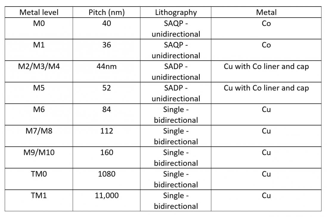
This past January, I had postulated that 2017 would be the “Year of the Embedded FPGA”, as a compelling IP offering for many SoC designs (link). As the year draws to a close, I thought it would be interesting to see how that prediction turned out.
The criteria that would be appropriate metrics include: increasing capital investment; increasing customer adoption; support for a diverse set of applications; and, an emerging set of standard product offerings to accelerate adoption. To be sure, qualified test vehicles fabricated on multiple foundry process nodes are also crucial, as is a solid methodology flow for design synthesis and physical personalization.
If you have been following eFPGA technology, you have no doubt seen recent press releases highlight the growing investment and the customer endorsements. In addition, previous Semiwiki articles have described how eFPGA features are addressing both high-performance and low-power requirements, as well as the ease with which the IP block is connected to the pervasive AMBA bus protocols (link, link). So far, the prediction is looking pretty good. 🙂
The last metric – the introduction of standard product offerings – has received less attention, perhaps. To gain a better understanding of the eFPGA product strategy, I recently met up with Aparna Ranachandran, Tony Kozaczuk, and Cheng Wang at Flex Logix. I asked how their technology offerings are evolving, as the customer interest grows.
Cheng indicated, “A key requirement is to address the applications where programmable eFPGA functionality also incorporates significant memory storage. Many customers are seeking a product that optimally integrates SRAM within the eFPGA logic tiles. They do not intend to invest a lot of resource in physical implementation – i.e., designing and floorplanning SRAM blocks adjacent to the eFPGA IP. These customers want a flow from their HDL description through synthesis to an off-the-shelf eFPGA product with programmable logic and memory.”
“To that end, we will soon be releasing an integrated design for silicon qualification, as a standard product.”, Aparna highlighted.
Tony added,“With lots of customer input, we have selected a combination of programmable logic capacity and array storage that will span a wide range of upcoming customer designs. We are leveraging the existing HDL synthesis flow support that provides block RAM’s in the output netlist, inferring the array topology from the HDL model. Our EFLX compiler maps each BRAM in the synthesis netlist to a corresponding configuration of SRAM macros integrated in the eFPGA IP.”
The use of Block RAM’s is the standard representation for synthesizing and implementing arrays for commercial FPGA products – so, this flow is a natural extension for eFPGA IP.The initial Flex Logix programmable logic + array offering is illustrated below.
Aparna is the lead designer, and provided a description of some of the technical features:
The overall flow for realizing the eFPGA logic + memory design is illustrated in the figure below.
The initial front-end EFLX analysis step provides customers with resource estimates, for both the programmable logic LUT usage and the array macro utilization. The subsequent steps complete the physical personalization, including the array macro connectivity.
“Our customers are seeking silicon-proven IP products – this offering will expand the application base to designs requiring integrated storage.”, Cheng said. (For specific customers who are interested in a unique integrated configuration, the Flex Logix team would assist them with preparation of the flow input descriptions shown as “optional” in the figure above, as well as the IP physical implementation.)
So, it looks like the eFPGA technology market is indeed expanding to offer customers with product(s) that will accelerate adoption, combining complex logic and storage requirements with a well-defined implementation flow. This past year has indeed been the “year of the eFPGA” – it will be interesting to see what 2018 brings.
For more information on the Flex Logix logic + array offering, please follow this link.
Have a Happy Holiday season!
-chipguy
Six years ago I first interviewed Stephen Crosher, CEO and Co-founder of Moortecas they were in startup mode with some new semiconductor IP for temperature sensing, and earlier this month I attended their webinar all about embedded in-chip monitoring to get caught up with their technology and growing success. Ramsay Allen is their VP of Marketing and he talked about how their business started out in 2005 based in the UK, focused as an IP supplier of Process, Voltage and Temperature (PVT) sensing.
Stephen Crosher, Ramsay Allen – Moortec
Stephen presented the bulk of the webinar and introduced the need for embedded in-chip monitoring:
FinFET transistors became widespread starting at 22nm and continuing into smaller nodes because compared to planar CMOS technologies it is offering lower leakage, lower operating voltages, higher silicon density, faster speeds and improved channel control. With the increase in density come new challenges of thermal hot spots, electromigration causing reliability issues, and leakage concerns. Even packaging costs become an issue as you can spend between $1 and $3 per watt consumed in the SoC.
As voltage supply levels scale ever downwards then chip engineers need to design for worst-case IR drops and account for increased resistance values in interconnect. There is even an industry segment on the high-end that is mining for Bitcoin, and their chip performance is bound by power delivery and air conditioning costs, so being able to run your chips cooler is a big financial benefit.
Smaller process geometry nodes like 28nm and below have reliability issues to contend with like NBTI (Negative Bias Temperature Instability) where the Vt value shifts over time, so IC designers need to know how far Vt values have changed during aging. Trying to reach timing closure is now complicated by process variations within a single die where one chip region has a unique PVT corner, while another chip region is operating in a different PVT corner:
Mr. Crosher shared a use case from AMD on their Athlon II Quad core CPU, designed at 45nm where they placed thermal sensors in each of the cores and then distributed the workload across the cores based upon the thermal readings from each core, making sure that no one core became too hot, balancing the core reliability.
In the second use case the challenge was to optimize voltage scaling by measuring the power and speed of each IC, then finding the lowest functional voltage possible, saving the unique settings in each device. Moortec even supports Adaptive Voltage Scaling (AVS) in a closed loop format by placing multiple Voltage Monitors (VM) or Process Monitors on each chip:
There was even a use case where an enterprise data center used embedded chip monitoring to do real-time temperature monitoring to allow power optimization, provide a failure prediction of devices, and to protect each CPU by providing a safety shutoff limit. This is a big deal for data centers because they are such large consumers of power from our electrical grid, and their projected growth is staggering. Today, about 2% of our total electricity is taken by Data Centers, and with a CAGR of 12% these power stations will produce more greenhouse gas than airlines by 2020.
The actual monitoring IP from Moortec has both hard macros and a soft PVT controller as shown below:
This IP is already used in many nodes: 40nm, 28nm, 16nm, 7nm.
The number of monitors and their placement is dependent on each unique application, so the engineers at Moortec are happy to give you a hand on where to place Process, Voltage and Temperature monitors.
Summary
The challenges in our modern SoC chips can be met through the use of PVT in-chip monitors. You could try and create your own IP to do this, or just task the experts that have been doing this for over a decade and re-use their silicon-proven monitoring IP.
Q&A
Q: How do I test your IP?
A: Thermal – a reference is required to test accuracy, so this is done by probing on die, and we have test chip programs to ensure no self-heating. There’s only a .003C temperature rise from adding a sensor. Yes, we have correlated silicon versus simulation data.
Q: Where do you store info coming out of PVT sensors?
A: Register sets in the control block. You would store output in your own SoC design, not in our IP.
Q: Is the voltage monitor immune to Vdd fluctuations?
A: Our voltage monitor is looking at Vdd supply across its full range, designed to be immune to ripples, and it’s robust.
Webinar Recording
To view the entire 42 minutes webinar, visit this link.
Aldec continues to claim a bigger seat at the table, most recently in their attendance at SC17, the supercomputing conference hosted last month in Denver. I’m really not sure how to categorize Aldec now. EDA company seems to miss the mark by a wide margin. Prototyping company? Perhaps, though they have a much stronger focus on end-applications than a general-purpose prototyping solution, witness also recent attendance at the Trading Show in Chicago this year, where they were showing off platforms to support high-frequency trading (HFT).
In at least some of these applications it isn’t even clear that the Aldec solution is limited to prototyping. In low-volume applications (for example HFT), the Aldec boards may well be the final implementation. This is certainly apparent in some of the solutions they talked about at SC17: a DES code-breaker, a ViBe motion detector and a solution for short reads alignment in genome sequencing, as close to live applications as you can get.
Starting with the DES code breaker, I’m sure Aldec isn’t planning to enable hackers, also DES is no longer considered a secure encryption standard. However, this demo is a good example of using Aldec boards to build accelerators. In this demo, they show off a brute-force code-breaker to crack 6144 56-bit DES instances in ~20 hours using their HES-HPC accelerator with 6 Xilinx UltraScale chips. That’s a pretty powerful demonstration of the level of computation that is possible in an FPGA-based accelerator.
A more directly applicable demo shows off ViBe-based motion detection. ViBe is a popular method to detect and subtract background in video sequences, making it especially important in detecting moving objects in video, for example other cars or pedestrians. In this example, they are processing 1080p video at 39 frames per second and using the same HES-HPC platform to run ViBe background subtraction in real-time. This would naturally be useful in ADAS and autonomous driving applications and would be equally useful in security/surveillance applications and autonomous drone applications as just a few examples.
Their third demo is one of the coolest uses of an accelerator I have seen, to accelerate gene sequencing. As I understand it, today sequencing a whole genome in one shot is still a challenging (and expensive) problem. Sequencing methods more widely available for production applications tend to do something called short reads, reading a small set (a few hundred base-pairs) at a time (base pairs being pairs of the famous nucleotides A, C, G and T). These must then be mapped to a reference genome through a process of approximate string matching. This way the sequencer flow can build up a reconstruction of the actual genome sequence.
Of course, there are several challenges in this task. First, human DNA (as an immediately interesting application) has about 3 billion base pairs. Second you don’t expect an exact match to the reference genome. Mutations of various kinds are part of what makes us different and are a contributor to many ailments. There are also repeats/ redundancies in the genome. Matching has to take account of all of these potential differences. But at the same time, it has to be super-accurate. Human genomes are 99.9% similar across all types of humans so there’s really very little room for error.
ReneLife, a faculty enterprise of the Indian Institute of Science in Bangalore, has developed a solution (ReneGene) to sequencing short reads that is faster, more accurate and significantly more cost effective than existing solutions and they have done so building on an HES-HPC platform. They compare an earlier software version of their solution with existing solutions and show it is more accurate and faster when running on a supercomputer cluster supported by a GPU cluster. OK, but hardly scalable to mass usage (at an estimated cost of $400k/year). Then they ported their solution to an HES-HPC implementation, running at an annual cost of less than 1% of the supercomputing solution, and it runs faster still. That sounds like a very compelling option for mass-market deployment.
I have to believe there are many more applications that could benefit from massive acceleration, for which the economics of an ASIC solution (and the skill-sets required) don’t make sense. FPGAs are a perfect fit in this cases and ready-made accelerator boards are even better (qv Raspberry Pi, Adafruit, etc.). Aldec seems to align very well with these needs. Perhaps we should call their products application-specific accelerator platforms. ASAP – not bad and certainly closer than EDA to the mission that is apparent in their trade-show and customer footprint.
With the advent of the Internet-of-Things (IoT), Industry 4.0, Cognitive Computing, and autonomous vehicles and robots we are seeing an unprecedented number of systems-on-a-chip (SoCs) going into mission-critical applications. To accomplish the complexity of these applications, SoCs are being manufactured in leading-edge processes where manufacturing tolerances are being pushed to their limits. Not only are the devices more complex, but the processes required to manufacture them have more subtle defects mechanisms than in the past. All of this has led to designs with exploding test data volumes and associated testing costs that could threaten their viability.
The test and electronic design automation (EDA) industries have done a brilliant job so far to keep up with Moore’s Law through the introduction of testing technologies like SCAN synthesis, ATPG, Built-in-Self-Test (BIST), and Embedded Deterministic Test (EDT). EDT has scaled to well beyond the 100X range for data compression, but the demand for more compression continues as test pattern data volumes are driven by more complex design structures, greater combinatorial depth, more complicated clocking schemes, and the use of new fault models appearing at advanced nodes. Mentor, a Siemens business, recently released a new white paper that touches on these points and introduces their next generation of test compression dubbed Tessent VersaPoint Test Point Technology.
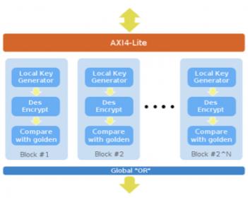
VersaPoint is a hybrid of Mentor’s Tessent TestKompress (TK) and Tessent LogicBIST methodologies that combines EDT and LBIST. EDT provides the high-quality test needed for mission-critical requirements while LBIST is used for in-system testing. Both these technologies (EDT and LBIST) use something known as ‘test points’ to improve the overall testability of a circuit. If you remember back to IC-Test 101, to be able to detect a fault on a given node, you must be able to both control and observe that node. Test points are extra logic inserted into a circuit that lets you do just that. See figure for examples of typical logic used for both control-type and observation-type test points.
Previous to VersaPoint, the insertion of test points for both EDT and LBIST required a two-step process. VersaPoint enables a one-pass process in which test points for both types of tests are added concurrently. Both the analysis the insertion steps for the test points can be performed on a gate-level netlist either before or after scan insertion. While this makes for a simpler test flow, more importantly it also provides for better test compression results.
As evidence of the better compression achieved, Mentor added the following table of 15 designs ranging in size from 1.4M gates up to 23.3M gates with an average size of 7.3M gates. The average compression ratio for these designs when using standard EDT methodologies is 46X. However, with the new VersaPoint test points, the average pattern count reduction achieved for these designs is 5.2X vs only 3.9X when using EDT test points. This may not seem like much but when you look at the compression achieved from using the VersaPoint test points you get a whopping 240X compression as compared to a 46X compression from EDT test points alone. That’s a lot!
One key aspect of adding test points is to minimize any negative effects of the test points on circuit timing closure. Mentor has added several features to support this including the ability to exclude test points from any false and multi-cycle paths using a functional SDC file. Test points can also be excluded from critical paths extracted from static timing analysis and the number of control-type test points added to a single path can be limited to a specific value.
While VersaPoint test points give great results for Stuck-At Faults (SAF), they are also effective for all other types of fault models as well. The white paper has tables showing similar if not better results when using VersaPoint test points with Transition Delay Fault (TDF) models. VersaPoint test points also have benefit when used with so-called ‘low-power ATPG’ algorithms that try to reduce switching activity. These low-power ATPG algorithms tend to create higher pattern counts which can be mitigated by using VersaPoint test points.
All in all, the new VersaPoint capability seems impressive and with the new era of Mission-Critical SoCs that are coming to market, it’s good news that Mentor continues to attack the test problem. Making sure SoCs for these types of designs are manufacturing defect free has got to be high on a system design company’s list of priorities, which bodes well for Mentor’s Tessent family of products.
See also:
White Paper: Improving Test Pattern Compression with Tessent VersaPoint Test Point Technology
Mentor Tessent Products web page
CES 2018 will start soon and will be held on January 9-12 in Las Vegas. If you plan to go to Vegas, don’t miss CEVA-powered smart and connected products and demos! CEVA’s product portfolio includes DSP IP cores (the smart) and RivieraWaves IP platforms supporting wireless protocols, like WiFi and Bluetooth (the connected).
DSP is by nature ubiquitous, as DSP core can process any type of digital signal, but CEVA has developed solution for specific applications like intelligent vision, advanced imaging, computer vision or ADAS processing to name just a few. Let’s review the various demos proposed by CEVA at CES 2018.
Intelligent vision – neural network based applications running on a CEVA-XM vision platform silicon. You can read more about CEVA-XM family in Semiwiki: “Intelligent Vision in (Almost) Every Application”
Computer vision – CEVA-XM powered products demonstrating 3D vision, depth sensing, and real-time stitching for 360 degrees video. In semiwiki: “Computer Vision in Mobile SoCs and the Making of Third Processor after CPU and GPU”
Advanced imaging – image enhancement for smartphones and surveillance systems based on embedded photography DSP. The quality of the photography is certainly one of the top three criteria for a consumer selecting a smartphone and chip makers are integrating more and more complex image processing chain. After extraction of raw digital data from the CMOS imager, and running of (single or dual) camera image signal processing (ISP), you must address the key elements of intelligent vision processing, namely 3D vision, computational photography, visual perception, and analytics. The CEVA-XM4 and its associated tools and libraries combine to deliver a comprehensive vision IP platform to do it.
Automotive – ADAS processing by a leading automotive CEVA customer. You may want to refresh your memory with this Webinar from CEVA: “Enabling mass market ADAS applications using real-time vision systems”
AI speaker – far-field multi-microphone reference platform for smart speakers and voice activated IoT devices. In this excellent blog from Bernard Murphy, “CEVA and Local AI Smarts”, you will get a status about AI, as Bernard consider that “For the first time, AI methods not only lived up to the promise but are now beating human experts. (In deference to AI gurus, neural nets have been around for a long time. But their impact on the great majority of us took off much more recently.)”
Smart headset – active noise cancellation software solution for headsets and earbuds, powered by CEVA Audio DSP. Several blogs have been written in Semiwiki to describe DSP solutions addressing voice and audio, here is the last update: “Active Voice” in Semiwiki.
Audio over BLE– high-quality audio streaming over BLE, demonstrating CEVA Bluetooth 5 low energy working in tandem with CEVA Audio DSP. If you want to know more about Audio over BLE, I recommend you read this article from Franz Dugand, Director of Sales and Marketing, connectivity BU, CEVA “Bluetooth Audio Streaming is Everywhere and Improving”
Wireless connectivity – complete connectivity solutions for IoT gateways using CEVA’s Wi-Fi 802.11ac and Bluetooth 5. CEVA’s wireless connectivity IP are coming from RivieraWaves acquisition. Numerous blogs have been written in Semiwiki about wireless connectivity solutions from CEVA, including “4 Reasons for Bluetooth 5 Adoption in IoT”
NB-IoT solution – complete reference design for cellular IoT based on CEVA-Dragonfly NB1 platform (see above picture). The platform is Single-processor, licensable NB-IoT solution for cost- and power-sensitive LTE IoT devices. You will learn more about CEVA-Dragonfly in this blogin Semiwiki.
Please note that CEVA will exhibit at suite No. 2938 in the Westgate Las Vegas central tower and that access to the suite is by invitation-only. According with CEVA, demo and meeting appointments are filling up fast, so contact them now (you can go here) and a member of their team will be in touch to schedule your meeting.
By Eric Esteve fromIPnest
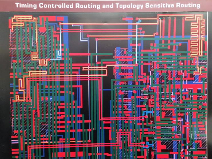
The year is now 1991 and in search for a more peaceful life we decided to move to Canada. At that time, very few companies had advanced flows in VLSI but Ottawa having BNR, Northern Telecom, Mitel, etc., looked to be the most promising place. After a few hiccups in finding a job, I landed in MOSAID, a small company with35 people at that time. From Motorola with central CAD who qualified all tools and PDKs with local CAD who built specialised tools, to a company with no CAD at all. MOSAID was a small design services company specialized in DRAM. One division was doing only design services the other was designing and building very advanced and specialized engineering testers for memories. I was in a new country, new company, new language and no CAD support. This was great opportunity to start fresh using all previous experience in tools, flows, etc. MOSAID Semiconductor division did not have a layout team at all, so I accepted the position of supervisor of the new IC Layout group with 5 members. We were using Apollo machines and Chip graph software for layout, hardware & software coming from Mentor Graphics. Slow and limited for layout but very good for circuit design as it had the “case frames” system in schematic entry, something Cadence does not have until today.
The layout was tedious as no PCELLS available. We had a good coding guy in our team, Karl Skjaveland, who already started to add some automation in AMPLE code bindkeys, device generators, etc. Soon enough Mentor came up with the new revolution in their software called IC Station,this was the answer to Cadence OPUS environment. New software meant that we needed to develop new bindkeys as we had specialized memory application to support and we already had our setups in Chipgraph. We got lucky, we got the visit of Ed Fisher, the engineering manager for IC Station development. Ed came to Ottawa and spent a week with the layout team observing how we work, learnt why we do what we do and took our bindkey to productized them as part of IC Station new releases. We were very happy that we contributed to next generation tool. With this new IC Station came new additions, tools that had automation in mind and I wanted my team to try everything. We invited Glenn Thorstensen to Ottawa and tried the new IC Plan, IC Block, IC Route, IC Verify and all other new software available for layout. Unfortunately, none was useful “as is” for memory design and we did not have CAD to help customization, but we did learn a lot about other IC Station features related to these tools.
We learnt the most important thing,thinking FLOW is more important than thinking one tool solution.
Around 1995 another revolution came to VLSI layout, IC Craftsman, the first “shape based router”. The company was Cooper & Chan Technologies (known as CCT) and they came to DAC to present it. A very refreshing move was to bring early advance users to demo the tool. This is how I became friend with Jack Wild and Paul Mason. I really liked this router but I was in Mentor Graphics environment and there was no integration between the 2 platforms. You needed to export and import GDSII to use the router, but this did not stop me get one copy. First time we used the router in a 16Mb SDRAM central channel and we finished the work in 1 week instead of 3 with all the setup time. This was very good for MOSAID but not good enough for me! Following year, I spoke with 2 important people in CCT, Mr. Chan and Dave Reed. I explained them that a router without a placer built by the same team is only half job. Mr. Chan started to look at options and solutions for devices and cells placement and the following year at DAC we sat together and reviewed progress and options. I remember the debate on device generation “with” or “without” contacts…
The idea was that the router can add the source/drain contacts! The problem is that in 1997 CADENCE bought CCT for the router and they wanted to kill this new baby placer, they already had 5 of their own placers. I am coming to DAC to see the new placer, called Dev Place, and there is no demo for it, nothing… CCT booth became resting area… Went to Dave Reed to find out how can I see the final product but learnt that the software is on the way OUT. The only option was to gain users support and force CADENCE to let it fly to see if it is more successful than other internal products or not. At that DAC I convoked all my industry friends to go to Cadence and ask for a demo of Dev Place. John Cohn brought almost all IBM participants at that DAC for demos. My friends from Intel, Motorola, AMD, all Israelis I knew went for the demos and we won! Very excited I came back to Ottawa and ask Cadence country manager, at that time, Nick Deeble for a copy of the software. Guess what, it was not even on the list for software to sell. So we had a “special deal”: I get the software AS IS, with no maintenance, no future updates, no bug fixing and no support. We payed the money and got the software. Charlie Houck, the AE who came a year earlier to install IC Craftsman came again to help us get Dev Place up and running. I was lucky to get people who knew their “stuff” and were exited to help. Now was time to show my management in MOSAID why we spent the money.
I started to work with one of my colleagues Andrew Holban to figure out how can we integrate IC Craftsman and Dev Place into a flow including IC Station. We worked together before in MSIL and he followed me to Canada. His job was not really CAD but LayCAD, meaning helping layout with automation but nobody else was available at that time. After a IC Craftsman success, we had a few brainstorming discussions with the whole layout team and we came out with a flow. Andrew called it C.A.R.IN.A. – Cadence Automated Routing Interface Application. Below is what Andrew built: a text based user interface capable to help a layout designer plan, place and route 500+ standard cells from and into IC Station with 100% clean DRC and LVS at 350 nm process level. How?
Using a plain text file on the screen, through questions & answers the script was providing the building box of the required block: size in X and Y directions, side on which you want the pins to be in order or not, and numbers of rows for placement.
This box was exported through GDSII to CCT environment together with the design netlist and a library with all cells involved. Kind of LEF, DEF and .lib in the digital world.
The script exported back the placement and routing into IC Station through GDSII and ran the verifications required, in that case was still Dracula.
We promised management that with C.A.R.IN.A. we will finish a block of 500+ cells for a memory periphery (layout in rows) in 1 day compare with the hand crafted 5 days best results. On the first demo Andrew finished in 2 hours and the managers were very pleased! But we did not stop there. Knowing the router speed is based on number of vertices the tool has to evaluate we built abstract cells, but smarter than the digital libraries. They only had routing layers on top modified to let only potential routing areas free and having minimum vertices per polygon. We merged all metals where routing was not available. You can see this concept explained in my book. At step 2 in the new release of the “flow” the script was using the abstract library in CCT and coming back to IC Station the reference points were replaced with the real layout. We got down from 2 hours to 20 minutes…
I want to highlight 2 important factors in this success:
The management believed in our ideas and capacity to deliver. They invested the money for a “bleeding edge tool” and allowed Andrew to be out of production for 4 months.
I was lucky to have Andrew in my team. I was just the enabler and the instigator. He wrote, implemented and released C.A.R.IN.A. alone!
Remember that we did this 2 years before Cadence succeeded to even integrate them in Virtuoso environment. The new Virtuoso Custom Placer (VCP – Dev Place) and Virtuoso Custom Router (VCR – IC Craftsman) was used to build the ACPD flow in a unified environment. How is this for pioneering?
Parts 1-3

I attended Oski’s latest Decoding Formal event a couple of weeks ago and again enjoyed a largely customer-centric view of the problems to which they apply formal, and their experiences in making it work for them (with Oski help of course). From an admittedly limited sample of two of these events, I find them very representative of the high-end of formal application, what you can do when you build significant internal expertise or bring in experts like Oski. These events also highlight the kinds of property-checking problem that are attacked at this level, falling outside the range of formal apps (today) and in some cases outside what you might even consider normal usage. I’ll get to that last point in a subsequent blog.
The event opened with a keynote given by Dan Lenowski (Sr. VP Eng. and cofounder of Barefoot Networks). Dan started with a quick overview of the anatomy of a shared network switch (apologies in advance to networking experts – what follows is my non-expert view of the domain): per-lane receive MACs and ingress forwarding pipelines, in the middle packet buffering and queueing, then again per-lane egress forwarding pipelines and transmit MACs. Dan talked about verification challenges for each separately.
Formal plays the biggest role in datapath verification (the central block), where it shines in dealing with combinational complexity across variable-sized packets and variable line-speeds, particularly in verifying the queue arbiter (no surprise to formal experts). Here they use it to model:
Saurabh Shrivastava (Sr. Mgr. at Cavium) spoke next on a methodology for formally verifying software-defined networking (SDN) silicon, an important topic for networking devices today. Saurabh pointed to OpenFlow as a reference standard for SDN where the control layer and forwarding layer are separate and the control layer manages multiple devices/switches. This can obviously be managed, optimized and reprogrammed to handle multiple possible use-cases, today and in the future, such as IoT use-modes and SD-WAN. So highly configurable, but it can’t be slower than hard-wired solutions and, because it is configurable, verification has to deal with a very complex configuration space, across all of which it has to deliver top performance. In other words, a great fit for formal.
Saurabh went into a lot of detail on their formal methodology and I don’t want to steal his thunder (watch the video), but I will say I was impressed by the discipline in their process. They follow a full test-planning and tracking methodology which would be familiar to any simulation-based verification team. They have intensive test-planning and tracking, a common Makefile and regression framework, coverage review, the works. Assertions, constraints and cover properties are all comprehensively reviewed by the team and tracked as verification progresses. Coverage reviews are as detailed as testplan reviews and they mark off what is covered by formal since it then does not have to be covered in simulation.
Saurabh illustrated with 4 designs ranging from relatively simple to more complex, with I thought an illuminating discussion on how they proceeded through managing the complexity of the formal problem in each case. This is when formal runs out of space/time or gets to an inconclusive result on the raw problem and you have to start thinking about cut-points, black-boxes and abstractions. Saurabh started gently with an IPv4 header checksum generator block. They tried proofs with and without an inserted bug. Formal found the buggy case, slowly, on the full RTL but the clean case run was inconclusive. They ran through 3 stages of abstraction to get down to runs where both the bug was found quickly and the clean case returned a proof. In subsequent examples, they used symbolic values, reset abstraction, data coloring and symmetries to get to closure. Good case studies on dealing with complexity management.
You can check out Oski’s Decoding Formalvideos HERE. (The December video was not yet posted at the time I wrote this, I assume it will be soon.)

I recently was introduced to a white paper written by John Stabenow, Director at Mentor, a Siemens Business, that gave an excellent overview of things to consider before launching into the design of an IoT edge project. John starts the paper with a quote from Pliny the Elder (A.D.23-A.D.79) who said, “The best plan is, as the common proverb has it, to profit from the folly of others”. This reminded me of a saying from one of my past supervisors who told me that “common things happen commonly”. Most mistakes have already been made by others and rather than repeat them we would all be wise to learn from their folly.
With that wisdom in mind, this is a white paper you will want to keep close at hand as the checklists contained in it can be used as a quick reference the next time you start a project. John breaks the planning task down into several areas including:
Each of these areas have multiple sub-areas to be considered and John does a good job of walking the reader through them. I’m going to highlight a few because these always seem to be the ones in my experience that ended up biting the teams with which I have worked.
The first thing that I’ve seen is that teams get confused about the purpose of the planning process. The idea is not to generate a bunch of documents because someone says you must. The planning process is meant to make you really think through what it is you are going to do and how you are going to go about doing it. If you must write something down, that will force you to start thinking through the alternatives to bring clarity to the documents.
The second thing that usually gets lost until much further into the project is the concept of a test plan. Done correctly, the test plan is part of the specification process. Not only do you specify what the system should be doing but you must also specify how you will test that the specifications have been met. If you address both these documents at the same time, you’ll usually find that your specifications aren’t nearly as clear as you thought them to first be. This is especially important if you are working on a design that has some safety implications and John does a good job of discussing some ways in which requirements can be captured and tracked across the design process using tools like Mentor’s ReqTracer.
A third thing that tends to get short shift in smaller companies is infrastructure and automation. An ounce of prevention here is worth a pound of cure later. Simple things like standardizing on project directory structures and file naming conventions can make things a lot simpler when it comes time to automate steps and archive the design when complete. I would lump into this category the use of version control or version management software. Ideally version management should be used for any files that are used by the design, including design data, test benches, documentation, automation scripts and even meta data about versions of CAD tools that are being used for any part of the design. It may seem silly to use version management software for automation scripts, but when you are deep into the design and a script change breaks everything, you will be wishing you had the previous version of that script that you knew worked correctly.
The last thing I pulled out from John’s white paper was the idea of defect tracking and how it relates to requirements management. As already mentioned, if you are working under a safety standard, you often need to prove how you track and manage defects. If you are designing in a modular fashion, testing of design blocks should be happening as each design block is implemented and bugs found during that process should be tracked against their associated requirements, specifications and versions of the block’s implementation. The last thing you want to do is fix a bug and then not have the fix get merged in with the rest of the design.
There is so much information in the white paper I can’t begin to cover all of it in this article. Hopefully I’ve given you enough of a feel that you’ll pull a copy for yourself and give it a read. I think you’ll agree with me that it’s a keeper. The next time you start a project, pull this white paper out and give it a quick read. It will really make you think about your next steps.
See Also:
White Paper: Preparing for an IoT Edge Project
ReqTracer web page
Tanner Tools web page
eBook – Custom SoCs for IoT: Simplified – Available for Free Download

The Consumer Electronics Show (CES) is in its 50th year believe it or not! The first one was in New York (1967) with 250 exhibitors and 17,500 attendees. Portable radios and TVs were all the rage followed by VCRs in 1970 and camcorders and compact discs in 1981. This year there will be 3,900+ exhibits and an estimated 170,000 attendees with augmented reality, high resolution audio, IoT, and all electric concept vehicles taking us into the future of electronics and more importantly semiconductor design.
CES is the world’s gathering place for all who thrive on the business of consumer technologies. A high-level business event that touches all industries, it’s the place where business gets done. A platform for innovators of all sizes to build their brands, every major technology company on the planet participates in CES in some way — by exhibiting, speaking, sponsoring, attending or holding co-located events and business meetings.
Cadence will be at CES again this year showing the Tensilica line of DSP based processors for audio, automotive, IoT, and consumer products. Tensilica started with SemiWiki in 2011 and continued up until their acquisition by Cadence in 2013 for $380M in cash.
You can find a Brief History of Tensilica HERE in case you are interested. I did predict a Tensilica exit (IPO) in 2013, close enough I would say. Currently Tensilica is everywhere: Mobile handsets, home entertainment, PCs and printers, automotive, Storage/SSD, IoT, and convolutional neural networks. According to Cadence, over 17 of the top 20 semiconductor companies use Tensilica processors to create more compelling and competitive products.
Based on the SemiWiki readership, the trending application for DSPs is artificial intelligence peaking with the disclosure of the Apple Neural Engine inside the A11 Bionic SoC. Apple did not disclose the specs but it certainly behaves like a DSP running at up to 600 billion operations per second.
The iPhone X facial recognition is a prime example of AI inference and training on the edge which of course is powered by the new neural engine. In my opinion this is the tip of the iceberg which will lead to handset health and wellness applications we first saw on Gene Roddenberry’s Star Trek in the 1960s.
Do you remember the tricorder? It’s coming to your iPhone, absolutely! As history has proven, where Apple goes others will follow, so you should expect an explosion of DSP based silicon for AI applications on edge devices. The cloud is already AI enabled with ASICS (Nervana/Intel, Google, and Groq), GPUS (NVIDIA and AMD), and FPGAs (Xilinx and Intel/Altera). Unfortunately, transmission speeds (WiFi and 4/5G) will never keep up with the demands of autonomous cars, robotics, handsets, etc… so the real action will be on the edge devices and that means DSPs, my opinion.
And if you want to see the future of edge devices CES is the place to be and Cadence would be a great place to start: Schedule a meetingwith our top executives at CES 2018 and see how the Cadence® commitment to current and future Tensilica® products meets and exceed your needs. Learn more about our products in neural networks, vision, and audio, and see how Tensilica processors continue to innovate and keep your products ahead of the competition. Visit our meeting room at CES 2018 and see our vision and audio demos and Tensilica DSP-based consumer products already in the market.