webinar banner AI 2026 v2

Thermal and Reliability in Automotive

Thermal and Reliability in Automotive
by Bernard Murphy on 06-12-2018 at 7:00 am

Thermal considerations have always been a concern in electronic systems but to a large extent these could be relatively well partitioned from other concerns. Within a die you analyze for mean and peak temperatures and mitigate with package heat-sinks, options to de-rate the clock, or a variety of other methods. At the system level you might rely on passive cooling or plan for forced air or even liquid cooling. These methods treat heat as more or less a bulk property to be managed. But that approach alone is breaking down in a number of modern applications, for which automotive (in ADAS and autonomy) provides good examples.

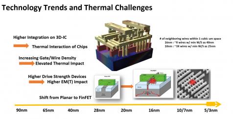
What changed? Ambient temperatures in a car (up to 150[SUP]o[/SUP]C) are a lot more stressful than mobile devices have to consider. This isn’t new but we’re now packing those mobile technologies and more into the car, with much higher safety expectations. That’s just to start. Automakers need higher levels of integration of heterogenous technologies, in part driving a trend to advanced packaging where we now have to consider not only thermal effects within a die but also between stacked die. System builders also moving much more aggressively to advanced processes because they need the performance and lower standby power. But this means gates and wires crammed closer together with more heat concentrated in smaller areas. Worse yet, FinFETS with their wrap-around gates are unable to dissipate heat as effectively as traditional planar gates.

FinFETs have higher drive strengths, which is good for performance, but into narrower interconnects which increases the risk of electromigration (EM), impacting device reliability. Local heating also accelerates EM, and it increases power consumption and risk of timing failures. Heat can cause mechanical problems. In 3D stacks, or 2/5D on interposer, also on the board, heating can lead to warping between layers (Toyota had a recent problem with cracking solder joints caused by thermal stress). None of this is acceptable in automobile safety-critical functions.

OK, you get it. We need to analyze thermal more carefully, but there’s another challenge. In product design we like to split our analysis into different domains: timing, power, thermal, EM, die-level, package-level, board-level and system-level. It’s just too hard to do it any other way, right? We do detailed analysis in one domain at a time and we handle inter-dependencies between domains using margins. But increasingly the margin approach is requiring impractical over-design. More importantly, the automakers/Tier1s are demanding more cost-effective high-reliability solutions, which can only be accomplished though co-design and optimization from the system down to the die (incidentally this is also driving closer collaboration between the semis and the OEMs/Tier1s.) Effective thermal analysis has to span all of these domains, though here I’ll just touch on thermal analysis from system to die and related mechanical analysis.

Using ANSYS products, analysis spans a wide range of technologies, from RTL power analysis and RedHawk thermal, up to computational fluid dynamics (CFD) to model cooling at the system level, and ANSYS/Mechanical to model thermal-induced warping. Many of these are multi-physics analyses, pulling together fine-grained data from multiple domains (thermal, fluid modeling, mechanical, …) to provide accurate analytics for potential hotspots, rather than the approximations inherent in a domain-by-domain approach.

ANSYS starts with profiling at RTL, these days often driven through emulation-based modeling, so you might characterize for power profiles (developed in PowerArtist) during OS boot versus 4K streaming. From this they develop block power profiles and then chip profiles based on the floorplan. RedHawk CTA then builds a chip thermal model (CTM) containing understanding of hotspots in that die. In a multi-die package these analyses can be combined to provide a package-level thermal analysis, combined with a mechanical analysis of stress (and potential warping) in that configuration.

Up at the system level, thermal models for each of the components (chips, voltage regulators, sensors, …) are combined in an Icepak CFD analysis to assess steady state and transient thermal profiles, including whatever passive or active cooling may be provided. Naturally this analysis is iterative; you model system-level thermal profiles and take this back to the die for refined modeling. That gives you improved data on EM and other risks across the die, to which you can respond with appropriate design optimizations. Which in turn should provide a more accurate handle on thermal-related failure rates across the system. I don’t know if anyone in the automotive value chain is looking at this yet but based on what I’ve heard about rising expectations in ISO 26262, I wouldn’t be surprised to see this kind of analysis become a requirement at some point.

You can watch the recorded webinar (delivered by Karthik Srinivasan, Sr. Corporate AE Manager in the Semiconductor BU at ANSYS) HERE. He covers a lot more detail, including local thermal effects and doing power/thermal loop simulations using SIwave and Icepak at the system level. There is also some interesting discussion on where these methods are important beyond automotive. Well worth watching.


RAL, Lint and VHDL-2018

RAL, Lint and VHDL-2018
by Alex Tan on 06-11-2018 at 12:00 pm

Functional verification is a very effort intensive and heuristic process which aims at confirming that system functionalities are meeting the given specifications. While pushing cycle-time improvement on the back-end part of this process is closely tied to the compute-box selection (CPU speed, memory capacity, parallelism option), the front-end involves many painstaking setup preparation and coding. As such, any automation and incremental checks on the quality of work for both the design and the embedded codes used for its verification should help prevent unnecessary iterations and shorten the overall front-end setup time.

UVM Register Generator
Register Abstraction Layer (RAL) was part of the Universal Verification Methodology (UVM) supported features introduced in 2011. It provides a high-level abstraction for manipulating the content of registers in your design. All of the addresses and bit fields can get replaced with human readable names. RAL attempts to mirror the values of the design registers in the testbench, so one could use the register model to access those registers. A RAL model comprises fields grouped into registers, which along with memories can be grouped into blocks or eventually grouped into systems.

Aldec’s Riviera-PRO™ verification platform enables testbench productivity, reusability, and automation by combining the high-performance simulation engine, advanced debugging capabilities at different levels of abstraction. In its latest release (2018.02), it introduces RAL support.

As illustrated in figure 1a RAL model automatic generation involves taking the register specifications of a design (Riviera-PRO supports either IP-XACT or CSV spreadsheet formats) and generates the equivalent register model in System Verilog code.

To better appreciate how this register model is used in the UVM environment, consider how it interacts with the rest of components in the verification ecosystem as illustrated in figure 1b.

The creation of register model is normally followed by the creation of an adapter in the agent, which makes abstraction possible. It acts as a bridge between the model and the lower levels. Its function is to convert register model transactions to the lower level bus transactions and vice versa. The predictor
receives information from the monitor such that changes in values in the registers of the DUT are passed back to the register model.

As register model is captured at a higher level of abstraction, it does not require knowing either the targeted protocol or the register type to be accessed. Hence, from the testbench point of view, one can directly access the registers by name, without having to know where and what they are. Instead, the Register Model stores the details of all the registers, their types as well as their locations. It is the responsibility of the RAL to convert these abstracted accesses into read and write cycles at the appropriate addresses and using bus functional model. This convenient approach also makes tests to be more reusable.

Another component in the ecosystem is the sequencing part as shown in figure 1c. Sequences are built to house any register access method calls or Access Procedural Interface (API’s). Users may categorize these API’s into three types: active (read, write, mirror), passive (set, reset, get, predict) or indirect (peek, poke). The registers are referenced hierarchically in the body task to call write() and read(). The commands peek() and poke() which are utilized for individual field accesses.

Unit Linting
Linting is a prerequisite for good coding practice. It is common to have this done at the end of system code completion prior to checking-in the release. Unit linting which was previously done as stand-alone from Active-HDL Workspace, has been integrated as part of Riviera-PRO User Interface. Launching unit linting from this Riviera-PRO dashboard can be done through selecting a new button that will run unit linting on the open file and display the violations back on the console. This integration lets designer to work on a design, do the simulations as well as run linting from the same interface. It provides cross-probing facility that cross reference the violation versus the affected line of code as illustrated in figure 2.

Productivity Improvements and Partial Support to VHDL 2018
Code elaboration takes time as well as memory. In this Riviera-PRO release memory footprint during elaboration is reduced by as much as 80%, while improvement in simulation speed of 25% is noted for System Verilog constraint random design and up to 10x faster for assertion based designs with multi-clocks.

Proactive partial support is also available to the VHDL 2018 extension, which is going through the formalization process. This includes handling the conditional analysis directives and inferring constraints from initial values of signals and variables.

Furthermore, less restrictions were imposed on handling these constructs:
– Optional component keyword after the end keyword closing component declaration
– Denoting the end of the interface list with an optional semicolon sign.
– Allowing empty record declarations or qualified expressions or signatures of formal generic subprograms in a generic association list.

I had the chance to talk with Louie De Luna, Aldec Director of Marketing to further comment on these recent updates.

Would the corresponding System Verilog codes automatically generated for the register models and their associated adapters correct-by-construction or need to be validated?
We generate the UVM-RAL from user’s provided spreadsheet (*.csv). Successful generation is highly dependent on the input quality. Once generated, it is correct-by-construction. The users do not need to review it and they can easily attach it on their testbench.

Can designers skip those units already passed unit linting when they do full design linting?
Unit linting provides facility to conveniently perform code checks while it is being constructed. Unit linting may have simpler rules compares with the full linting that requires different ruleset. Designers have option to include or exclude particular checks. Linting is good, but since too many rules may clutter the process these filtering options should help.

What reference point used for performance comparison and any plan to extend beyond this supported list when VHDL 2018 ?
The comparison made for Riviera-PRO 2018.02 release is with respect to 2017.10. We plan to fully support when the VHDL 2018 is formally published.

For more detailed discussions on these features please check HERE


DRC is all About the Runset

DRC is all About the Runset
by Daniel Nenni on 06-11-2018 at 7:01 am

EDA companies advertise their physical verification tools, aka DRC (Design Rule Check), mostly in terms of specific engine qualities such as capacity, performance and scalability. But they do not address an equally if not more important aspect: the correctness of the actual design rules.

Put bluntly: It’s not about how fast you check, it’s about what you check. To draw an analogy from a slightly different EDA domain: Designers can implement their RTL design in an FPGA device from vendor-A or vendor-X. Sure, there are differences between the two, but in essence, if the logic circuit fits in both devices and they are fast enough, either will do. What absolutely cannot be compromised is the correctness of the RTL code. If there are bugs in the RTL code, extra capacity and higher speed of the FPGA device will not help; functional verification is of the essence.

DRC is all about the runset
The same holds for DRC. One tool may run faster or take less memory than the other, but in the era of abundant and low cost cloud computing these are not critical factors any more. The quality of the check is determined less by the engine that runs it, and more by the correctness of the DRC runset code:

  • Is the DRC runset code correct? : Does it accurately represent the design rule intent?
  • Are the rule checks complete? : Does the DRC code cover all possible layout configurations?In practice the likelihood and severity of potential issues vary from case to case; broadly one can distinguish between the following three situations:
  • A physical design that is implemented in a mature technology that “saw” hundreds or thousands of designs already. In this case chances are that “holes” and bugs have already been (painfully) found in previous designs and have been fixed by the foundry. Using a 5-years-in-volume-production vanilla flavor process? – probably no need to worry.
  • A design that targets a relatively new technology, or a customized process flavor. There is a reasonable chance that the runset may still have inaccuracies or hidden “holes”. In this case it makes sense to inquire about the QA process of the runset, how many different designs have used the exact same process in production. If some design rules are customized and specific for this product or design style – runset verification can save a lot of cost and grief.
  • An early technology project: be it a foundry internal technology enablement project, an IP partner project, or an early access customer design team working closely with the foundry. In this case the runsets are clearly work in progress and must go through rigorous verification and QA process.The next obvious question is what tools and methodologies are available to address these issues and verify the DRC runset?Runset verification with DRVerify
    DRVerify is the leading commercial tool for DRC runset verification. Here is why:
  • Spec driven: The tool reads the foundry design rule descriptions (from any spreadsheet or text file) and allows to enter rules using a GUI. This rule description that represents the rule intent and is independent of a particular implementation is the source for creating the tests and the reference for their correctness and accuracy.
  • Powerful enumeration: DRVerify has a pattern enumeration engine then automatically generates pass/fail variations that exercise all boundary conditions of each design rules. The generated fail and pass cases cover all situations based on the design rule description (spec).
  • Flexibility: In addition to the automatic layout creation, the tool accepts additional layout patterns or actual design clips. Given such clips, the tool will automatically recognize the rules under test, and use them as seeds for further pattern enumeration.
  • The tool uses an internal independent spec-driven DRC engine that examines all these test cases, sorts them into fails and passes and places markers that are later compared to the markers created by the target DRC tool runset.
  • Coverage: DRVerify has a coverage measurement engine that analyzes all fail/pass cases and determines the level of coverage accomplished for each rule.
  • Detailed error report: Once the target runset or DUT (deck under test) runs on the QA test layout, DRVerify will run a comparison between each DUT marker and its own markers and measurements, and will provide a detailed comparison report, pointing to any mismatch or potential error in the runset.
  • No limitations: DRVerify is not limited to any given set of rules or specific technologies.
  • Tool independence: DRVerify is tool agnostic and can be used to verify any runset for any DRC tool or language.To learn more about DRVerify: DRVerify White Paper

Michelin Moving On: Deep Diving on Autonomous Driving

Michelin Moving On: Deep Diving on Autonomous Driving
by Roger C. Lanctot on 06-10-2018 at 12:00 pm

When it comes to autonomous mobility – things are changing awfully fast. A “deep dive” workshop at Michelin’s Movin’ On 2018 event in Montreal (concluding today) dug into the issue revealing hopes and anxieties shared by executives culled from a wide range of industry constituencies. The overall sense of the room was that autonomous technology is coming – perhaps sooner than some think but not as soon as some have claimed or desire. All agree there is work to be done on the technology and the regulations and maybe even on public education.

Executives from Keolis (Andreas Mai), Bestmile (Lissa Franklin) and SAE International (William Gouse) led the group-based discussion with the help of Jason Thompson from Jigsaw. The debate focused on three key issues:

  • Approval
  • Certification
  • Monitoring

Approval – Innovation or regulation?

50 states in the U.S. 10 provinces across Canada. A myriad of jurisdictions spanning Europe. And every one of these governments has an idea how autonomous vehicle features should be addressed and regulated.

What is the right balance? Too much regulation can stifle innovation. Too great a focus on full-speed-ahead-innovation can increased safety risks. The participants attempted to answer these questions:

  • Do we need an approval process to put vehicles on the road?
  • What are the most critical components of an approval process?
  • How do you balance “innovation” against “regulation?”
  • How do you address liability?
  • Should aftermarket autonomous driving gear require approvals?
  • Who should bear responsibility?
  • National strategy or provincial/state strategy?

(A sampling of the responses is pictured above the headline of this blog from Post-It notes.)

Certification – What’s in the box?

Autonomous vehicles – whether commuter trains or SUVs require reams of data to test and improve algorithms. Companies in the space tend to be highly protective of algorithims and the datasets that populate them. One expert remarked that “I go to a lot of meetings with these companies, and when it’s time to share information, the room gets awfully quiet.

”That said, certification is becoming increasingly important to heighten consumer trust, improve safety and define what an autonomous vehicle is and where it can drive.

Experts spent time describing scenarios that could accomplish the goal of certification. Chief among them was the need to test, in the same way that crash test dummies are used to test products today. Car companies don’t want to share their specific details on enabling safety – what’s important is to know it works.

To get attendees thinking about certification, the experts asked seven new questions:

  • How do you balance “innovation” against “regulation?”
  • How do you certify an always-learning black box?
  • Should “transparency” be required?
  • How do you create “trust” for certification?
  • How does certification apply for commercial vehicles?
  • What kind of testing should be required?
  • How do you pursue the Good Housekeeping Seal of Approval?

The audience was split on the idea of opening the black boxes of proprietary IP. Some felt that creating transparency was vital for safety. Others felt it would cause fewer companies to innovate and compete.


Monitoring – Worth the (privacy) trade off?

Earlier this year, an Uber driver in Arizona was involved in a fatal crash involving a pedestrian. Part of Uber’s pilot program for autonomy, the driver was reviewing data on a tablet and hadn’t looked at the road for more than six seconds.

How does Uber know this? There were cameras in the vehicle monitoring the driver. What they didn’t do was warn the driver of the impending collision, or take action to avoid the problem. It appears the emergency braking was not engaged with the autonomous driving system.

How can monitoring – cameras, radar or thermal – make for a safe autonomous driving experience? Experts discussed the concept of monitoring in a broader context, expanding beyond driver monitoring to car monitoring or commercial vehicle monitoring. They asked what the role and value of monitoring – and touched on the trade off between safety and privacy.

Ultimately, the group identified a series of technologies and issues for the audience to discuss with these results:


This exercise got audience members dreaming about the future – particularly when it came to the potential for 5G technology. Ideas flew fast and furious throughout expert and attendee exchanges, and if there was one shared thought, it was this – this is a rapidly moving industry that’s thriving on big thinking, but at what cost and for what benefit?

Editor’s note: Thanks to Jason Thompson of Jigsaw for his moderation and for sharing his detailed notes. And thanks to Michelin and the event sponsors, of course.


Is This the Death Knell for PKI? I think so…

Is This the Death Knell for PKI? I think so…
by Bill Montgomery on 06-10-2018 at 7:00 am

It was 1976 when distinguished scholars Whitfield Diffie and Martin Hellman published the first practical method of establishing a shared secret-key over an authenticated communications channel without using a prior shared secret. The Diffie-Hellman methodology became known as Public Key Infrastructure or PKI.

That was a long time ago. Do you even remember 1976? If you’re over the age of 50 you likely recall some things about this era, but if you’re under 40, your knowledge of the ‘70s is probably stuff you’ve seen on television or read in history books.

In 1976 the USA average annual income was $16,000, gas was $0.39 a gallon, and the median price for a new home was $43,600. In the world of technology, Steven Jobs and Wozniak formed the Apple Computer Company and months later, Bill Gates registered Microsoft with the Office of the Secretary of the State of New Mexico. Matsushita launched VHS video recorders, and the first commercially-developed supercomputer – the Cray 1 – was installed in the US at the Los Alamos National Laboratory.

In 1976, the Internet didn’t exist, at least not in the way that it does today. There were no personal computers, no mobile phones – and of course no smartphones, It was a largely electro-mechanical, analogue world that was on the cusp of experiencing what over time was dubbed “the digital revolution.”

A technology guru who had gone into a deep sleep in 1976 only to awaken 42 years later would be shocked by the massive technological advances that have forever changed our planet. The guru would see a connected world with close to four billion Internet users, five billion mobile phones, and myriad applications that render global communication instantaneous. He or she would see a world with billions of connected things, with millions being added daily, extending well beyond consumer products to mission-critical business and government infrastructure. The 70’s guru would see that the very pillars of civilized society – nations’ energy grids, financial systems, and national security networks– all deeply ingrained and reliant on our connected world. And he’d also see a connected world constantly under attack by cyber criminals. He’d see the average cost of a data breach was $3.62m in 2017. He’d see nations under constant siege as enemy states and others work tirelessly to hack and destroy the digital foundation upon which we rely so heavily.

The world today would surely stun our tech guru, but what would absolutely shock him would to learn that virtually every person, place and thing on the planet, and every mission critical application is protected by 1970’s technology! PKI. And remarkably, enterprises and governments worldwide were paying an average $75/year total cost of ownership for each PKI-“protected” cryptographic unit (CU).
It begs the question, “how could our world have achieved so much in the way of technical advancement, without addressing the issue that can bring everything down?”

I won’t drone on about the perils of PKI – not the protocol, per se, but the vulnerabilities that a world full of fake and unrevoked certificates has created – but if you want to learn more I suggest you read Lipstick on the Digital Pig. What I do want to highlight is how one country – Singapore – is tackling the problem head on through an exciting initiative called Project GRACE.

A Tectonic Shift in Digital Security
I love the term “tectonic shift.” Its origins are rooted in geographic descriptions of the 15 or so tectonic plates that comprise the Earth’s crust. They are constantly moving, and when they move more dramatically, bad things happen – like earthquakes.

In the world of business, tectonic shifts are usually defined by the emergence of new technology that completely alters the landscape. Consider the tectonic shift from analogue to digital technology, which eliminated complete industries and ushered in the dawn of a new era. Apple, for example, obliterated the portable, personal music listening industry (remember the 1970s “Walkman?”) when it introduced the IPod.

The Government of Singapore – which is ranked #1 in the world in the IAC International E-Government rankings – is leading the way by creating a tectonic shift in digital security. Through Project GRACE, it will completely eliminate the many threats posed by PKI by completely erasing the dated Diffie-Hellman scheme from its digital equation.

GRACE has been entered in the co-sponsored US NIST and Homeland Security 2018 Global City Teams Challenge, an event which this year is focused on Cybersecurity. The GRACE initiative is described as follows:

“The present Public Key Infrastructure (PKI) is known to be inadequate for the current scale of the Internet and the situation is exacerbated with the advent of IoT. Project GRACE (Graceful Remediation with Authenticated Certificateless Encryption) implements a security architecture using an advanced form of pairing-based cryptography called Verifiable Identity-based Encryption (VIBE) to provide a simple, scalable and secure key management for the cloud services, the IoT and indeed the Critical Information Infrastructure (CII) which are otherwise vulnerable to the extant and new cyber-physical attacks.”

One of the partners in GRACE, the University of Glasgow, is the lead agent in a city project to secure all smart meters over public wi-fi networks using the certificateless approach (i.e. no PKI) inherent in GRACE.
GRACE is led by Singapore-based QuantumCeil which describes the projects deliverables, as follows:

  • Provide a simple scheme where it is difficult to commit errors of implementation.
  • Provide a scalable scheme to address very large networks (centralized, distributed or mesh – billions of entities) at a great reduction in complexity – O(N) over PKI – complexity O(N2).
  • Provide a secure scheme rooted in hardware with counter-measures against the crippling side-channel attacks [author’s note: this eliminates threats due to critical hardware vulnerabilities in modern processors, such as those exposed inMeltdown and Spectre].

The time has come for our connected world to migrate from PKI and embrace security technology and cryptographic schemes designed in this era for this era.

I just sent a text to the 1976 technology guru. He agrees. Do you?

p.s. the GRACE system and its operation are certifiable to ISO 27001:2013.


20 Questions with Wally Rhines

20 Questions with Wally Rhines
by Daniel Nenni on 06-08-2018 at 12:00 pm

When I first started blogging in 2009 my sound byte was, “I blog for food” and the first lunch invitation I received was from Mentor Graphics CEO Wally Rhines, we have been friends ever since. Wally has an incredible mind with a memory to match, coupled with his charm and depth of experience I would easily say that Dr. Walden Rhines is the most interesting man in the semiconductor ecosystem, absolutely.

In this series of blogs I hope to capture Wally’s experience in enough detail to publish it as an autobiography. Hopefully the SemiWiki community will get involved and help with questions, comments, and critiques, for the greater good of the semiconductor ecosystem…

A Winding Path to the Semiconductor Industry

Gainesville, Florida in the 1950s was a small town of 25,000 people that doubled in size during the school year. There was almost no place to work except at the University so most of my peers had at least one PhD parent on the faculty. Competition was fierce as situations (like the daughter of the head of the Math Department competing with the son of the head of the Physics Department for top scores in high school courses) raised the level of intensity.

My father was a professor and a traditional engineer, as was his father so when it came to discussion of career choices, the conversation was short. “I think I might like to be a lawyer”, I might say. “Engineering is great preparation for law school”, my father would reply. Or, if I suggested the medical profession, there would be a similar answer. Variants of this discussion were followed by more than a dozen visits to the leading engineering schools in the U.S. until he concluded that the University of Michigan had the best undergraduate engineering program. And so, that’s where I went.

While my father was pleased with my decision to affiliate with the Chemical/Metallurgical Engineering program, he was less enthusiastic about the love I acquired for computers. Michigan was the first university to acquire an IBM 360 mainframe and had a close relationship with IBM. Bob Arden’s Math 273 course attracted a lot of people I came to know later, like Sam Fuller (later head of R&D at Digital Equipment and CTO at Analog Devices), David Liddle (Founder of Metaphor….) and Fred Gibbons (founder of the company that developed pfsWrite, the first widely accepted word processor for the TRS 80 and Apple computers). Math 273 required us to complete four computer projects including a program to execute the Newton/Raphson convergence approach to find functional values of zero for an equation; little did I know that this basic algorithm would be fundamental to all the SPICE simulations I ran in the years ahead.

Sam Fuller and I joined the same fraternity and embarked upon various contests to see whether our brains or our livers had greater endurance. At one point, we decided that sleep was just an escape mechanism so we decided to eliminate it, with less than beneficial consequences.

As graduation approached, the intensity of the Vietnam War increased. In February of our senior year, President Johnson announced an end to automatic deferments for graduate students unless they were married, which Sam was. Marriage struck me as much too extreme an alternative (since I didn’t know anyone I wanted to marry) but I managed to find a program that let me go on to grad school if I spent the summer at Fort Benning “pushing Georgia” with push-ups as my Drill Sargent yelled at me. Choice of a graduate school was a switch from my undergraduate experience. Getting into good graduate schools wasn’t that difficult so I only applied to Stanford and U.C. Berkeley. Previous fatherly advice of, “If you’re good enough to go to graduate school, you’re good enough to get someone else to pay for it”, came back to haunt him as he lobbied for U.C. Berkeley as the real engineering school rather than the “science oriented” Stanford. Graduate schools provided the funding back then so the choice was mine. Sam Fuller, who was number one in the Michigan Engineering class of 1968, was being recruited vigorously by MIT and Stanford so, after many beer-laden discussions, we concluded that Stanford was the place to go. We rented an apartment while Sam’s wife finished her degree at the University of Maryland and we entered the world of semiconductors and computers at Stanford. Sam chose Prof. McCluskey as an advisor. I chose Dave Stevenson, who was granted a major DARPA contract to investigate III-V compounds.

Craig Barrett, who was a traditional metallurgist, decided to diversify from his background and become involved in semiconductors. Dave’s contract was the perfect opportunity. So Craig joined my PhD committee, along with Gerald Pearson, one of the group that developed the transistor at Bell Labs. Craig was the closest thing that Stanford had to an expert in electron microscopy, so he dutifully helped me analyze precipitates that were formed during the diffusion of zinc into GaAs to form light emitting diodes. As I made my way to the end of the research, Prof. Pearson told me not to worry about a job. He would take care of it.

Sure enough, Pearson was good to his word. When I told him I was ready, he picked up the phone and called Morris Chang (one of his former graduate students) at Texas Instruments. He did the same for Shang-yi Chiang my fellow lab partner who had the same advisors and later became head of R&D for TSMC. We both went to TI to begin a career in the semiconductor world. A few months after I arrived at TI, Morris was promoted to manage the entire Semiconductor Group. That ultimately led to an association that I value to this day.

20 Questions with Wally Rhines Series


When FPGA Design Looks More Like ASIC Design

When FPGA Design Looks More Like ASIC Design
by Bernard Murphy on 06-08-2018 at 7:00 am

I am sure there are many FPGA designers who are quite content to rely on hardware vendor tools to define, check, implement and burn their FPGAs, and who prefer to test in-system to validate functionality. But that approach is unlikely to work when you’re building on the big SoC platforms – Zynq, Arria and even the big non-SoC devices. It would simply take too long to converge functionality and performance. As usual, expectations keep ramping up – 400MHz performance, shorter design cycles and more designs per year, driving more reuse but still needing to meet the same regulatory and/or safety requirements. Sounds a lot like ASIC/SoC demands (except for GHz speeds in ASIC). Unsurprisingly, FPGA designers are turning to similar flows to manage these demands.


The design steps should look very familiar: planning, IP verification, full design static and formal verification, simulation, synthesis, implementation and hardware debug. Like the ASIC folks you may want a second-source option, in which case this flow needs to be able to target multiple FPGA platforms.

Planning is common in both domains, but here it must be much more tightly tied to pre-silicon functional verification. If you have to signoff to DO-254, ISO 26262, IEC 61508 or other requirements, you already know you have to demonstrate traceability between testing and specs, and completeness of testing. Which means you need linkages and as much automated correlation as possible between documents, testing activities, bug tracking, testing coverage, static code compliance metrics, and so on.

Many FPGA designers are already familiar with static verification, an elaborated version of the linting of 15+ years ago. This is still a mainstay and a requirement in many FPGA flows (DO-254 for example mandates a set of coding-style rules). Equally important here are clock-domain crossing checks. A big FPGA may host 10 or more clock domains and 10k+ clock domain crossings. If you don’t use static analysis to find and check these, you face a lot of painful debug on the board. The better static checkers do a comprehensive job in finding all crossings, while reducing the cases you have to analyze to a digestible format.

Formal verification is a newer entrant in FPGA verification but is gaining ground for some fairly obvious reasons. One is getting to acceptable code coverage. All big designs have unreachable code – from disabled or forgotten functionality in legacy or 3[SUP]rd[/SUP]-party IP. You can’t hit this in testing no matter how hard you try, but it’s still going to damage your coverage metrics unless you flag the code to be excluded. That’s not always so easy, especially if you don’t know the code. Fortunately, there are formal methods which will search for unreachable code, and will automatically create those exclusion commands.

Formal adds more capabilities through “apps” for the formal novice, such as looking for inaccessible states in FSMs or design exploration apps which will help you probe characteristics of your design without need to setup complex testbenches. In general formal can be a very valuable complement to simulation, for what-if experiments and when you want to be sure something can never happen, say in a complex control system where multiple FSMs are interacting (that’s a topic for more advanced formal users, but remember this if you run into such a problem).

The heart of verification in these flows is still simulation, which has evolved a lot from earlier simulators. Now it has to be mixed language, Verilog, VHDL and SystemC, modeling all the way from TLM through RTL and gate-level. These are big designs running at least some level of software on ARM cores, so you need all the acceleration you can get through multi-core and other techniques.

For testbenches these days you should be looking at UVM along with (SystemVerilog) assertion support and management, because you should be using assertion-based verification anyway but also because your IP and VIP will be loaded with assertions. And your simulator should provide strong constrained-random support with an excellent constraint solver, since you’re going to depend heavily on this for coverage.

Something that may be new for some FPGA teams is the need for good VIP (verification IP) in your verification plan. A lot of what you will be testing with interacts with standard protocols – the many flavors of AMBA, PCIe, USB and so on through the alphabet soup. VIP provide proven models for the testbench to simulate traffic under many possible conditions. You’ll need these not only for testing functionality but also for performance testing. Will your design hold up under heavy traffic?

You also need a very good debugger, which now has to support protocol transaction views in addition to the traditional signal waveform kinds of view. You don’t have the time or probably the expertise to figure out what’s broken in a protocol at the signal level; the right place to start looking is at the transaction level. Incidentally you really need for the same debugger to support simulation, formal and static verification, for ease of learning certainly but also for integration between the different types of verification and coverage.

Finally, what can the flow vendor do to help you in post-silicon debug and better still, bring that debug data back for drill down in the flow you used to verify pre-silicon? Again the FPGA vendors provide logic analyzer capabilities here but likely not as well-integrated with the pre-silicon flow. So that’s consideration if you think you may need to do some tracing through the RTL. When looking for a debug solution it should be easy to use and integrate easily with the verification flows for quicker turnaround times.

The flow needs a good synthesis engine. Why not just use the FPGA tools synthesis? You can; naturally they understand their underlying architecture as well as anyone, so you can expect they will do a good job in optimizing your design to the hardware. But they’ll freely acknowledge that they don’t synthesize to competing platforms and they don’t have the depth and breadth in synthesis technologies that you’ll find in the big EDA companies. Which is why they work with those companies to enable those EDA tools to also optimize on their FPGA platforms with high QoR, advanced debug and deep verification.

I haven’t talked about any preferred solution in this blog; ultimately you should decide that for yourself. But I think I have described a reasonable checklist you might want to use to grade solutions. One possible solution is described in this webinar.


Are memory makers colluding against China?

Are memory makers colluding against China?
by Robert Maire on 06-07-2018 at 12:00 pm

Maybe OMEC is the new OPEC? A bargaining chip in June trade show down?

China has started an apparent investigation into pricing of DRAM memory with Samsung, Micron and SK Hynix as targets. We find this somewhat coincidental given the current trade issues. Memory pricing has been unusually strong for a very long time. Much longer than any previous period in the usually volatile memory market. The tight supply demand and therefore pricing in a normally volatile and less profitable memory market begs the question of whats going on?

Is it simply that memory makers have finally gotten intelligence and self control? Is next generation memory so hard to make that supplies are limited by technology? Or is it potentially a more nefarious reason like the collusion that China may be searching for?

If it is collusion, whats wrong with that? It may not be illegal or even wrong for memory makers to collude. Maybe not to set prices but maybe to set supply, which in turn will support pricing, much like the oil market.

The other, potentially more plausible answer is that China may be looking to preempt the trade showdown looming from the Trump administration on June 15th and June 30th.

If China can claim that the US and others are conspiring against it then perhaps they have more of a leg to stand on in trade issues. Maybe the investigation could be a bargaining chip to be bargained away in trade negotiations. Go easy on us or we will bust your companies for colluding against us.

There is also clear precedent of anti trust behavior in the DRAM market in the US. From 2002 to 2006 there were investigations and guilt found for violating violating the Sherman anti trust act in regard to DRAM pricing for Samsung, Micron and SK Hynix.

DRAM price fixing history link
Could this simply be history repeating itself? It could. The impact of the real truth behind memory makes a significant difference in the fortunes of the memory companies and trade issues.

Looking for leverage
It would seem clear that China wants leverage in coming trade talks and raising the specter of anti trust creates a FUD factor (fear uncertainty & doubt) that helps its position. Price collusion is very plausible given the industries history, so it appears to be very solid.

It is the timing that makes us suspicious but there is nothing that can be proven as it is a legitimate concern.

We would not be surprised to hear that the Chinese are dropping their price collusion investigation in return for some concession from the US and others.

What are other concessions that Chinese may ask for?
China already asks for, and gets, “technology sharing” on the part of the selling company. In other words the price of doing business in China is giving away some of your trade secrets to the customers and would be competitors. The trick is to give away useless information or nothing of true commercial value. Many companies in the tech space have made an art form of this. Seemingly giving away things without really doing so. Intel’s first foray into China was to locate a packaging factory which gave away little if any of the company’s true crown jewels.

Given the recent ZTE scare, China may push a lot harder to get access to real, true hard core leading edge technology to reduce dependency on the US and others. We are certain this is the case as ZTE made them painfully aware. Showcase and “make believe” technology sharing will likely not suffice any more.

Is OMEC the modern day OPEC???
Maybe the US and Korea (and Japan too for Toshiba) governments should get together and form OMEC (the organization of memory exporting countries). The reason that OPEC can collude is that “sovereign states” (not companies) are immune from Sherman anti-trust.

Maybe we don’t understand the power and leverage of producing memory.

If oil was the driver of the 20th century global economy through transportation then memory is the driver of the 21st century economy through “big data” and other data driven applications. They are both truly global commodities that are central and the life blood of new economies. China is a new economy that needs memory perhaps as much or more than it needs oil.

Ratcheting up the rhetoric
One of the problems we see is that both sides seem to be ratcheting up both rhetoric and ammo for some sort of trade show down. As we have said before, this could be a big game of chicken but it becomes harder to back down and unravel all the rhetoric and come to a reasonable accord. Much as was the case with the North Korean issue, we see no resolution in sight for the China trade issue. We would feel much better if there were a hint of progress but so far we don’t see it.

No collusion?
Like and Unlike presidential politics, there appears to be little evidence of collusion among DRAM makers other than the circumstantial evidence that prices remain high and supply remains low. As is the case in US politics, the facts never stopped anyone, as China could still indict any or all DRAM companies, as enemies of the state, with or without evidence and hold them hostage and linked to trade talks. After all it appeared that ZTE and its ongoing existence was being held hostage from China’s vantage point.

The stocks
We still are very concerned about both June 15th and June 30th as things are incrementally more complicated and ratcheted up in the past day given the DRAM collusion investigation. We still think semis and semi equipment are squarely in harms way in a trade war and this DRAM issue proves the point perfectly.

While over the longer run we see little impact on the stocks there is risk of companies giving too much away to China to “pay to play” in the Chinese market.

The short term risk in the stocks remains the headline risk in June which just got a bit worse.

We still like Microns stock, and if anything, this issue just serves to underscore the immense value in a memory supplier to the global economy. Both Samsung and Micron have already seen that value reflected in their earnings if not their respective stock prices. Micron’s stock remains especially cheap.

The semi equipment names remain at risk of being sucked into the vortex of the trade dispute as they have yet to be directly involved or called out by name. The first equipment company to get caught in the trade tussle will take down the entire group. It will not be good to be the test case. If we can get past the trade talks without semi equipment getting caught up it will be a minor miracle.

In the meantime we look forward to the Trump administration publicly saying that there was “no collusion” in DRAM pricing in response to China’s allegations…


John Lee: Market Trends, Raising the Bar on Signoff

John Lee: Market Trends, Raising the Bar on Signoff
by Bernard Murphy on 06-07-2018 at 7:00 am

I talked to John Lee (GM of the ANSYS Semiconductor BU) recently about his views on market trends and the ANSYS big-picture theme for DAC 2018. He set the stage by saying he really liked Wally’s view on trends (see my blog on Wally’s keynote at U2U). John said these confirm what he is seeing – a trend to specialization, some around new applications like autonomous vehicles, some around traditional platforms like mobile and HPC and some around new technologies like 5G.


REMINDER: Make sure you register for your free I Love DAC pass by June 8th!

He noted some other trends, one to what he calls reaggregation, especially in moves for pure-play foundries to ramp up in-house ASIC services. Another is in system vendors getting close (or close again) to silicon: Cisco acquiring Leaba Semi, Amazon acquiring Annapoorna Labs, Bosch building their own foundry and Facebook and Google clearly being very active as judged by semiconductor design job postings in Indeed.com. In all cases, chip design activity is being driven increasingly by system companies who are seeing more advantage/differentiation in dedicated rather than general-purpose solutions.

In John’s view, these shifts are triggered by hot applications moving to more complex processes and packaging, and increasingly becoming sensitive to system-level design constraints. He cited for example automotive suppliers, traditionally very conservative on process but now moving to 7nm and already starting to engage at 5nm to integrate more complex compute (AI, 5G, imaging, …) onto silicon. For similar reasons, 3D packaging is picking up, in FPGAs, network, mobile and image sensors, all to scale beyond Moore’s law.

With these moves come more challenges, one being the sheer size of the design analysis task. To take one example in John’s domain, at 16nm a typical power grid might be modelled with a billion resistors; at 7nm you now have to handle 10-20B, up 1-2 orders of magnitude. The criticality of problems is also rising. FinFETs are driving higher current density into narrower interconnects and razor-thin voltage margins in these processes amplify risks in timing, yield and reliability.

John said that at 7nm they’re seeing breakdown in the standard approach to managing timing and voltage margins, judging by the calls they’ve had from a near full-house of high-end customers. These companies have told them that they are losing important yield to performance problems they thought were covered. They’re finding they need tighter timing accuracy near the margins than traditional variability methods can offer, but MC-SPICE just can’t handle the volume of paths that need to be checked.

Meanwhile, mobile and crypto-currency applications are pushing the power envelope even harder. In 5G, serdes frequencies run above 50GHz. At these frequencies noise-coupling is no longer simply capacitive; you also have to consider induction and you can’t limit analysis to nearest-neighbor only. Thermal effects become more important; between thermal and higher FinFET drive into thinner interconnect, EM risk goes up. And when you stack die, thermal problems increase, adding potential mechanical problems – warping between die and on the interposer.

The industry has developed a lot of good tools to attack these different concerns pointwise, for example PTSI for signal integrity, RedHawk for power integrity, Calibre for manufacturability and FX and RedHawk for reliability. However these tools are siloed, each excellent in its own domain if you can rely on margins to model inter-domain variability. That’s like modeling a problem in a box with margins as the sides of the box. You can analyze one problem really well inside that box, but the analysis can’t extend beyond the sides. This works well when the box completely surrounds the problem. But if you have to make the box really big to meet that goal, the design may not be viable – too expensive, too slow, too power-hungry or too unreliable. On the other hand, if you shrink the box to meet product specs, at least some behavior will spill beyond the edges of your analysis; you don’t even look at some realistic behaviors which could lead to failure.

At DAC, ANSYS is going to talk how to more completely analyze the problem space in all dimensions by removing the box, something they call “beyond signoff”. A reasonable approach must continue to depend on the learning already built-in to best-in-class tools, which means the solution needs to be open and extensible. It also must manage vast amounts of data from all of these tools to enable the kind of true multi-physics analytics common today in other domains, such as design for aircraft engines. This is only possible if you can leverage best-in-class technologies and computational sciences. And the solution needs to enable designers to innovate beyond the democratized processes, IPs and software platforms that we all have use, letting them build on their expertise to differentiate in power, performance, cost and reliability.

To learn more about what ANSYS plans for DAC 2018, click HERE.


Being Intelligent about AI ASICs

Being Intelligent about AI ASICs
by Tom Simon on 06-06-2018 at 12:00 pm

The progression from CPU to GPU, FPGA and then ASIC affords an increase in throughput and performance, but comes at the price of decreasing flexibility and generality. Like most new areas of endeavor in computing, artificial intelligence (AI) began with implementations based on CPU’s and software. And, as have so many other applications, it has moved up this chain to the optimal trade off point for both flexibility and performance. However, unlike cryptocurrency mining, AI utilizes constantly changing algorithms and architectures, which are often specific within a given application area.

AI when implemented for ADAS, search, VR, voice recognition, image analysis etc., calls for unique solutions in each space. The inability of a general-purpose ASIC to best handle a variety of applications has created a road block to the adoption of ASICs for AI. Yet, this leaves potentially huge gains in power efficiency and performance on the table. eSilicon just announced an offering they call neuASIC that promises to solve this problem and give developers of AI ASICs much more flexibility and a well thought out methodology for implementation. Before their official announcement at the Machine Learning and AI Developer’s Conference, I had a chance to talk with eSilicon’s Carlos Macián, Sr Director of Innovation, about their new approach.

The key insight driving this approach is that while there is a common notion of what an AI ASIC looks like, the parallel processing elements in the system are most likely to vary based on the application. There’s benefit to dividing the system up so there is a chassis consisting of IOs, data and control path interconnect, a CPU for control and internal and external memory. In addition, there is an array of AI tiles which have the AI neural network processing elements and their local memory. These AI tiles and the array that connects them are the most likely elements to change with new system requirements and new applications. Of course, the base elements may need to change too, but in general they will prove more durable and hence more reusable.

eSilicon is a pioneer in applying 2.5D technology to building efficient and high-performance designs. It comes as no surprise that they are using this technology to create their solution for AI based systems. They divide the design up into two parts, the AI core die and the ASIC Chassis die. The ASIC Chassis contains scratchpad memory, CPU, NoC based scalable control path, 3D data path interconnect, bus interfaces and external memory IOs. The AI core die consists of AI tiles custom designed for the AI application that the system is targeting. Together they go into a package along with HBM to create a full system for AI.

Designers are not left on their own to design each of the pieces. eSilicon provides their Chassis Builder software, AI tile cells and the IP for the ASIC Chassis itself. They offer Giga cells and Mega Cells that contain full AI subsystems and AI primitives respectively. Putting all this together they have everything needed to design and implement optimized ASICs for AI, and this offers the ability to modify select portions for future designs as algorithms and approaches change and improve.

They also have two very interesting pieces of IP that further help improve system performance. The first is their Word All Zero Power Saving memory. It offers 1RW (1 read or 1 write access per cycle) along with an 80% reduction in power. The power for all zero word read/write is 20% lower than WC read/write. This is useful with the sparse matrices used in AI. These benefits come with a very nominal 2% overhead (16Kx64) compared to conventional memory. The second is their Pseudo Four Port memory. They use a foundry 8T bit cell and perform 2 read and 2 write per cycle. They can be configured as 2R2W, 1R2W, and 2R1W multiport memories.

As AI becomes more prevalent in silicon design we are seeing an explosion of innovation in system implementation. While nobody is standing still – witness the GPU companies adapting their silicon to meet AI market needs – it’s interesting to see the synthesis of several technologies like 2.5D, advanced data/control paths, AI tile design, etc. used to create flexibility, improved turnaround time and better performance. eSilicon has a large team working on AI IP and system integration. The results look impressive. For more information on eSilicon’s neuASIC look at their website.