It used to be that at the mention of libraries, people would think of foundry PDK deliverables. However, now a host of factors such as automotive thermal requirements, nanometer FinFET processes, near threshold voltages, higher clock rates, high volumes, etc., have dramatically changed library development. These factors have led to new library formats such as Liberty Variation Format (LVF) and Composite Current Source (CCS). Both of these formats incorporate more accurate modeling approaches than their predecessors AOCV and POCV. However, achieving this higher accuracy comes at the price of increased processing requirements to generate models.
The newer models are more statistically oriented. CCS includes slew rate and load dependent timing information. The net result is a requirement for many more SPICE runs and, of course, more computation. Chip designers now often have library needs that go beyond what the foundry supplies, shifting the burden for library characterization to the chip design side.
Recently Silvaco broadcast and posted a webinar that addresses the issues around library characterization facing semiconductor companies. In the webinar Silvaco’s Bernardo Culau pointes out the rapidly increasing number of PVT corners that need to be modeled to ensure design success. Among the drivers he cites extended temperature ranges, temperature inversion effects, the trade-off between power and operating voltage, and high temp burn-in corners. According to him, these and other considerations can necessitate simulating each cell in the library at hundreds of corners.
The real issue with library characterization is that each project may have different needs for libraries and varying capabilities needed for generating the needed models. Of course, the largest semiconductor companies can keep a fully staffed group dedicated to characterization with plentiful tool licenses and compute farm access. This luxury is not available to smaller companies or those with less frequent library characterization requirements. Relying on library providers for project or customer specific characterization can be expensive and delay projects. Companies that have specialized characterization needs, but that occur only occasionally, are faced with a difficult choice.
It can be expensive to maintain the staff and resources in-house for infrequent characterization needs. Also, if it is only done periodically it is hard to maintain the expertise needed to ensure the best results. One of the main thrusts of the Silvaco webinar relates to potential solutions to this problem for a wide range of companies. Silvaco has a unique mix of capabilities, including tools, professional services and access to the needed compute resources.
For smaller companies, it does not make sense to keep on hand the number of license keys necessary for rapid library characterization. Characterization calls for short duration, high volume tool licenses. Silvaco offers their SmartSpice simulator that is well suited for this task and they have developed business models that make sense for a wide range of companies. In the webinar Silvaco also discusses several approaches to provisioning compute resources. They include on-site, Silvaco servers and cloud services such as AWS or Google Cloud.
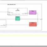
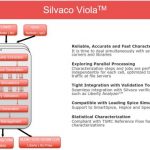
The centerpiece of their library characterization offering is the Viola product which is a complete solution for library characterization. It leverages parallel processing to accelerate the results. It also offers tight links to validation tools. Not only does it work with Silvaco’s SmartSpice, it also works with other leading simulators, such as HSPICE and Spectre. Lastly it is compliant with TSMC’s reference flow for statistical characterization.
Silvaco has thought through the requirements for library characterization for different types of enterprises and projects. Based on the webinar presentation, they are putting together an attractive set of business models, coupled with matched technical elements. To understand the challenges and their complete solution I suggest visiting their website to view the entire webinar.