Mentor continues to invest in conferences such as DAC, no matter the location, for which I am very grateful. They have a long list of activities this year but I wanted to point out my top three:
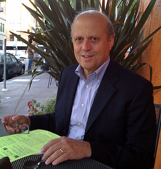
Wally Rhines has a talk in the DAC Pavilion which is first on the list. Wally’s expert industry perspective is the result of tireless research and endless customer meetings around the world and should not be missed. Wally will also be signing “From Wild West to Modern Life” books (last on the activity list) at the Mentor booth Monday at 5:00pm and Tuesday at 10:00am. There is a limited supply so I would get there early on either day. This is Wally’s first book, first book signing, and is your chance to get a piece of EDA history, absolutely.
FREE cappuccino from 9:00-2:00, and happy hour from 3:45-4:45 in the Mentor Booth. Hobnob with semiconductor professionals from around the world in the most casual setting. A great place to start and end your 56thDAC exhibition floor experience. I hope to see you there.
The 5G Myth vs. Reality Panel with Mentor, Synopsys and Cadence. Paul Mclellan and I were chatting about 5G at the Samsung Foundry event last week. His AT&T iPhone said he had a 5G connection while my Verizon iPhone said 4g. Identical phones different coverage. Marketing at its finest! This is an excellent opportunity to learn more about 5G from the semiconductor ecosystem, where electronics and 5G begins!
Activity List From Mentor Marketing:
The Design Automation Conference (DAC) is the premier conference for automated electronics design and verification technology. For 2019, DAC returns to sunny Las Vegas, Nevada at the Las Vegas Convention Center from June 2-5, 2019.
We’ve packed each day full of exciting activities and presentations featuring Mentor technical experts discussing the latest in cutting-edge design. You’ll find our experts in the conference program, in our booth (#334) hosting suite sessions and networking events, and in the Verification Academy booth (#617).
CONFERENCE PROGRAM
DAC Pavilion
Fundamental Shifts in the Electronics Ecosystem
MONDAY June 03, 10:30am – 11:15am | DAC Pavilion – Booth 871
Speaker: Wally Rhines – Mentor, a Siemens Business
Wally Rhines, CEO Emeritus of Mentor, a Siemens business, will examine major new market opportunities like AI/ML, automotive, 5G, etc. and how these markets will call for new design activity and the need for broader design tool innovation. He will also explore whether we are heading into a period of stability after three years of disruption or if the revolution will continue.
Straight Talk with Tony Hemmelgarn, Siemens Digital Industries Software CEO
MONDAY June 03, 11:30am – 12:00pm | DAC Pavilion – Booth 871
Moderator: Ed Sperling
Myth vs. Reality: What 5G is Supposed to Be, And What it Will Take To Get There
TUESDAY June 04, 11:30am – 12:00pm | DAC Pavilion – Booth 871
5G is trumpeted as the big enabler, providing massive throughput and a massive upgrade path for the mobile and mobility markets. It is a way for cars, phones and other connected devices to stream massive amounts of data to the cloud and back again. But 5G signals don’t travel very far, and they don’t penetrate objects. Devices built for this market will require extreme power management so they aren’t searching for signals constantly. Parts of them will always be on, which has an impact on design and reliability. And some parts, such as the antenna arrays, cannot even be tested using conventional means.
Panelists:
Neill Mullinger – Mentor, a Siemens Business
Peter Zhang – Synopsys
Ian Dennison – Cadence Design Systems
Paper Presentations
MONDAY, June 03
4.4 Electromigration Signoff based on IR-drop Degradation Assessment
8.4 Local Layout Effect Aware Design Methodology for Performance Boost below 10nm FinFET Technology
TUESDAY, June 04
18.4 A Lightweight Hardware Architecture for IoT Encryption Algorithm
WEDESNDAY, June 05
66.4 Virtual Methodology For Performance and Power Analysis of AI/ML SoC Using Emulation
69.4 Efficient Verification of High-level Synthesis IP
Posters
123.21 Metric Driven Power Regression – A Methodology based Metric Driven Approach for Power Regressions
123.25 River Fishing: Leverage Simulation Coverage to Drive Formal Bug Hunting
124.2 Comprehensive Analog Layout Constraint Verification for Matching Devices
124.7 Enabling Exhaustive Reset Verification in Intel Design
124.16 A Smart RTL Linting Tool with Auto-correction
124.25 Configurable Multi-protocol AUTOSAR-based Secure Communication Accelerator
125.12 Faster PV Signoff Convergence in P&R using RTD
125.14 Hybrid Methodology- An Innovative Methodology for Hierarchical CDC Verification
Moving Up in the World
125.17 Functional Safety on A-R-M CPUs
125.21 Tackling the Increasing Challenge of IR drop & EM Fails in Advanced Technologies with a Push Button Solution
EXHIBIT FLOOR
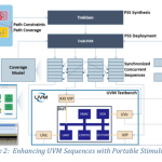
Mentor’s booth #334 is located on the west end of the exhibit floor. Check in daily for a host of technical sessions, networking events, panel discussions, a free cappuccino from 9:00-2:00, and happy hour from 3:45-4:45! You’ll also find Mentor verification experts in the Verification Academy booth (#617) for in-depth sessions on Portable Stimulus, UVM, and more.
Technical Sessions in the Mentor Booth
Each day, Mentor experts will be in the booth delivering technical sessions across:
- AMS Verification
- Analog/Mixed-Signal Verification
- Design & functional Verification
- Digital Design & Implementation
- IC Design & Test
You can view the complete list of technical sessions and pre-register here.
Expert Panel Discussions
Mentor experts will be moderating in-booth panels on both Monday and Tuesday directly following happy hour. Make sure to pick up a free glass of wine or beer before!
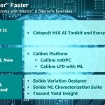
Design Smarter Innovations Faster using AI/ML and More with Mentor, a Siemens Business
MONDAY June 03, 4:00pm – 4:45pm | Mentor Booth #334
To enable our customers to deliver smarter innovations to market faster, Mentor, a Siemens business is actively delivering new solutions and use models that enable our customers to more readily develop AI-powered technologies. We are also integrating advanced machine learning algorithms into our existing tools to enable those tools to deliver better results faster. Come hear experts from across Mentor’s IC solutions portfolio describe what Mentor has to help customers deliver smarter IC innovations to market faster.
Panelists:
Ellie Burns, director of marketing, Calypto Systems Division
Vijay Chobisa, product marketing director, Mentor Emulation Division
Geir Eide, product marketing director, D2S Tessent Division
Amit Gupta, general manager, Solido, IC Verification Solutions Division
Steffen Schulz, vice president product management, D2S Calibre Marketing
Functional Safety in Isolation – Can Safety Be Collaborative?
TUESDAY June 04, 4:00pm – 4:45pm | Mentor Booth #334
As companies strive for greater levels of autonomy, more capability will be required of automotive ICs living at the edge, and the challenge of ensuring functional safety is exacerbated. The mass public trusts companies to deliver safe products to the market, but can the industry deliver on that promise given the demand for rapid innovation and complexity within the automotive ecosystem and supply chain? The scope of functional safety extends beyond the product boundaries to systems of interlinked devices representing the complete transportation network. From IP to automobile, each product plays a role in the overall functional safety of the transportation network. New paradigms and methodologies are required to ensure functional safety across all levels of the automotive ecosystem.
Panelists:
Yves Renard, Functional Safety Manager, ON Semi
Ghani Kanawati, Technical Directory of Functional Safety, Arm
Matt Blazy-winning, Functional Safety Director, NXP
Book Signing with Wally Rhines
Wally Rhines will be at the Mentor booth signing copies of his new book, “From Wild West to Modern Life”, Monday at 5:00pm and Tuesday at 10:00am.