
Radio frequency bandwidth has become a precious commodity, with communications companies paying top dollar for prized pieces of the spectrum. However, many radio bands are not often used efficiently. Many existing radio protocols exchange data on a fixed pair of frequencies, tying up those frequencies for other users. When this happens other users of those frequencies experience congestion that affects QoS. Then on the other hand there are often times in a reserved band where no licensed user is communicating at all. Years ago, it was recognized that if devices could more intelligently use the existing frequencies, efficiency could be dramatically improved.
The proliferation of wireless IoT devices is increasing crowding and the demand for improved efficiency. Additionally, it is no longer feasible to build a unique radio in a device to support each RF standard the devices requires. The solution to these problems is coming from software defined radio (SDR) combined with the intelligence to allow switching bands dynamically to utilize available areas of the spectrum. This new method of operation is called Cognitive Radio.
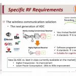
Cognitive Radio, which allows dynamic switching between bands to access underutilized spectrum, has recently been made feasible through advances in radio design. The challenge has been to build radios that can work on a wide range of frequencies. Moving as much of the RF processing to the digital domain is a major component of this solution. This is coupled with the adoption of Sigma Delta Analog to Digital Converters (SD-ADC) for the down-conversion.
When properly implemented SD-ADCs can reduce quantization noise though oversampling and noise shaping, dramatically improving the signal to noise ratio. Designers face many choices in the implementation the RF stage. Also, there is significant interplay between the digital portion and the RF stage, especially in tuning the baseband filters. Each wireless standard, such as GSM, LTE, 802.11, etc., has different signal requirements that must be accommodated in the radio.
Modeling and simulating the radio design is extremely important to ensure that it will operate properly once it is implemented and fabricated. SystemC and SystemC-AMS are proving to be useful tools in understanding the performance and behavior of radio designs. Choices need be made about design partitioning, parameter selection, software design, etc.
I recently had a chance to talk to Jean-Michel Fernandez, Embedded Systems Product Line Director, from Magillem about how IP-XACT can help this early design process. With SystemC models for each element in the design, it is easy with their MVP product to create a virtual prototype and then run simulation. This gives designers the ability to experiment with architecture, for instance relocating discrete RF components onto the SOC die. Also, the integration of software and hardware can be verified early in the design process. Later in the flow if the block level RTL has been brought into IP-XACT, the system RTL can be generated for synthesis, targeting an FPGA or ASIC.
With Magillem’s IP-XACT based MVP solution it is easy to assemble the receiver chain and then configure each component. Test benches can also be managed with MVP, so that everything needed for system level simulation is easily available. It is also straightforward to import legacy IP. MVP can automatically package existing SystemC code into IP-XACT.
Cognitive radio is one small piece in the increasing intelligence of electronic systems. It should significantly improve the overall efficiency and utilization of the airwaves. This will be seen by consumers in the form of lower communications costs, as well as in higher reliability and throughput. Magillem has information about their MVP product for managing design configurations and creating virtual prototypes on their webpage.


