The introduction of 5G communications support offers tremendous potential across a broad spectrum of applications (no pun intended). 5G is indeed quite encompassing, across a wide range of frequencies – the figure below illustrates the common terminology used, from low-band, mid-band (“sub 6G”), and high-band (“mmWave”) frequency allocation.
The massive MIMO antenna configuration for 5G offers high user volume, seamless mobile connectivity between towers, and extremely high availability – the latter is crucial for many applications, to be discussed shortly. The figures below illustrate a 5G antenna configuration, and specifically, the directed beam-forming radiation pattern as compared to the omnidirectional 4G pattern.
Although some commercial installations are already available in the mid-band spectrum, leveraging existing 4G LTE infrastructure, the promise of 5G is dependent upon the deployment of mmWave communications. The key characteristics of mmWave 5G are:
-
- ultra-reliability low latency communications (URLLC)
- enhanced mobile broadband (EMB)
For industrial IoT (IIoT) applications, a private 5G network may be deployed in support of robotic automation, sensor-based process monitoring, or operator-assisted procedures leveraging augmented reality (AR). These “fixed network” opportunities all rely on the URLLC features of 5G.
The majority of 5G development and capital investment is being applied to EMB applications, from consumer mobile telephony to the potential communication requirements of (Class 4/5) autonomous vehicles. The URLLC latency target is sub-1 millisecond to establish a connection, to improve upon “human-like reflexes” in an autonomous vehicle.
Parenthetically, although the pursuit of autonomous vehicle technology and the deployment of 5G EMB communications are extremely symbiotic, the two industries will proceed (somewhat) independently, driven by market demand and opportunity. On the one hand, autonomous vehicles may rely on local sensor data (LiDAR, radar, cameras) for real-time decisions, with vehicle logging and diagnostic data uploaded infrequently. In the most collaborative environment with 5G EMB, a rich set of vehicle-to-vehicle (V2V) and metropolitan vehicle-to-infrastructure (V2I) applications are envisioned. For example, a vehicle could communicate to the infrastructure the presence of a road hazard (e.g., road ice), an obstacle, or an approaching emergency vehicle, which would communicate that information to other vehicles for predictive decision making.
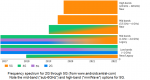
Note that the EMB applications envisioned for 5G are quite unique. Whereas a typical mobile consumer seeks high download “streaming” throughput, the bandwidth and low latency of mmWave 5G technology will lead to upload-centric applications, as well. The figure below illustrates the (potential) data transfer requirements for an autonomous vehicle, in full V2V and V2I communications mode.
Yet, the mmWave 5G transmission characteristics are drastically different than 4G LTE. The environments have led to the introduction of a myriad of 5G antenna design configurations, as well as connections to mid-band (and 4G LTE) networks – see the figure below.
Perhaps the most daunting challenge of 5G deployments is the metropolitan configuration, needed to support the V2I communications mentioned above (and provide consumers with the motivation to upgrade to a 5G-enabled phone J). Note that line-of-sight and non-line-of sight analysis is required for metropolitan mmWave 5G, accurately representing outdoor reflections. The figures below illustrate a metro cell radiation analysis model.
One of the most aggressive municipalities embracing 5G is San Jose CA. The city planning commission recently indicated a collaboration between the city and 5G carriers (especially, taxes and fees) with plans to establish 4,200 metro cells. Assuming a 65×65 cell configuration and a 150 meter distance between cells from the table above, that would cover roughly a 10km x 10km grid.
Yet, where will these antennas be placed? (There are both aesthetic and engineering criteria that will no doubt be part of this decision – I’ll focus on just the engineering aspects.) How will the carriers verify the appropriate beam-forming range and coverage?
Recently, I had a most enlightening discussion with Wade Smith, Applications Engineering Manager, High Frequency Electromagnetics at ANSYS. Wade impressed upon me the extensive amount of analysis required to evaluate 5G deployments, and how the breadth of ANSYS tools in the Multiphysics platform are applied to the problem.
“ANSYS has defined a full 5G analysis flow.”, Wade indicated – see the figure below.
Wade continued, “The scope of the analysis spans from the chip to a city. Correspondingly, the breadth of analysis utilizes ANSYS expertise in a range of domains.”
-
- chip element modeling (e.g., the RLC modeling tools from the recent Helic acquisition)
- signal integrity analysis
- electromagnetic radiation analysis (including specialized antenna radiation packages – i.e., SBR+)
- structural analysis
- thermal analysis
“The goal of the simulation is to evaluate the radiation pattern and spectral energy, in support of multiple users.”, Wade said. The figures below illustrate the beam-forming radiation pattern analysis from a base station to multiple mobile users.
“Structural analysis, too?”, I asked.
“To be sure.”, Wade replied. “5G antennas are housed in a radome that will be mounted on a wide variety of supports in a city, such as streetlights, utility poles, and the tops of buildings.”
“The mounting bracket will be subject to a number of mechanical forces, potentially exacerbated by weather conditions like high winds. With the critical role of V2I communications, the structural integrity of these antenna installations is paramount.”
“Of course.”, I said sheepishly. “What about the thermal analysis of the full chip-to-city model with ANSYS Icepak?”
Wade answered, “The ANSYS Multiphysics platform links Icepak and HFSS, for temperature-dependent antenna performance analysis. Although the 5G antenna is relatively small, and will integrate power management features that adapt to the time-varying load, the peak internal dissipation and radiated power is substantial. Icepak and HFSS will simulate the coupled electromagnetic and thermal solutions, and provide insights into the beam-forming radiation pattern and efficiency.”
“And, like the structural analysis, the antenna performance will be subject to external environmental conditions that need to be modeled. That ranges from the direct summer sunlight on the radome in Dallas to a frigid winter in Minneapolis – a Multiphysics-driven analysis approach is required.”
Wade showed some compelling examples on how the thermal analysis results were applied to the range calculations for typical antenna configurations. The first figure below illustrates the thermal analysis of the antenna array (with and without a heatsink). The second figure illustrates the effects of both the thermal analysis and external radiation interference on the 5G signal link margin – broadband interference noise will be present from over-the-air TV and radar signals. The impact of these effects on the 5G performance is significant.
“There will be a 5G deployment cost optimization effort undertaken by the carriers and the municipalities.”, Wade added. “The selection (with city approval) of the metro cell installations needs extensive Multiphysics analysis, to confirm the antenna radiation pattern margins. There’s a big cost differential between placing, powering, and maintaining metro cell antennas every 100, 150, or 200 meters.”
Looking at Wade’s example diagrams above, and thinking about optimally locating and verifying the range of 4,200 antennas in a complex model of buildings and roads in a city like San Jose, the analysis task is immense.
I live in a medium-sized city – population of 91,000 – and I will venture to guess that our city planning department has given little thought to developing an analysis model and initiating discussions with carriers on antenna configurations. It is early, I know, but I’ll attend an upcoming planning commission meeting to inquire. If your city has already been actively engaged in 5G planning, please let me know how it’s going in the Comments below.
I also intend to delve deeper into the ANSYS Multiphysics flow for 5G analysis in the earlier figure, especially with regards to the models used – a good starting point will be the ANSYS link here.
A number of whitepapers are available at this link, as well.
-chipguy