- Its “Complicated”- A 3 way Chip Relationship
- Competing for Wafers, Moore’s Law & Love
- Who’s Competing with Whom?
- All’s Fair
The 3 way relationship is more complex than it seems
On the surface it seems simple. AMD and TSMC compete with Intel making its own chips and TSMC making them for AMD. But below the surface the real competition is actually between Intel and TSMC for supremacy in Moore’s Law as that will determine chip performance, value and cost. Maybe not…Dig down another layer and maybe its a competition between the US and a foreign competitor. Dig a little deeper and its a clash of China versus the US.
So the competition is AMD & China Versus Intel? Or is it? Could it be Intel & AMD versus TSMC? Could it be Intel & TSMC versus AMD? Maybe all three.
Falling down the rabbit hole
Everything seems simple until you ask who TSMC’s biggest customers are. You might answer with the obvious choices. Apple, Huawei, Qualcomm, AMD and who else? You might answer Nvidia or HiSilicon, Marvell, Broadcom, Mediatek as number 5 but what if Intel was a top customer of TSMC? Well that strange revelation may actually be the case TSMC has been making chips for Intel and Intel has been short of capacity. Intel may be freeing up some capacity by off loading production to TSMC maybe a lot maybe a lot more.
A secret, convenient, affair?
Its not like either Intel or TSMC would want the “relationship” publicized. AMD might get mad at TSMC cheating behind their back and Intel might be embarrassed that it would have to go to its erstwhile competitor to get needed capacity…. much better to keep the “side” relationship quiet and discrete.
Is Intel really serious about Competing with TSMC?
Is Intel actually reducing “leading edge” capex?
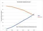
On Intel’s recent conference call they spoke about wanting to get back on a 2 or 2.5 year Moore’s Law cadence after stumbling around for 5 years with the 14/10NM transition. Sounds good but they may not be putting their money where their mouth is?
Intel announced a $500M increase in Capex which sounds like a lot of money but in the scheme of things is really just a bit over 3% increase from their current Capex budget, a fairly paltry increase. More importantly Intel said on their call that a significant portion of their Capex was going to increase capacity. We would interpret this “significant” capacity increase at likely more than 3% of their capex spend. The capacity increase is aimed more at 14NM and other non-leading edge geometries so the spend is not aimed at pushing Moore’s Law rather just making more of the same parts.
This suggests that the math means that actual Capex spend on 5NM and 7NM , leading edge, may actually be down after you take out the capacity spend.
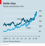
This hardly seems like a way for Intel to get back on a 2 to 2.5 year Moore’s Law cadence let alone catch up to TSMC which had a huge (much bigger than 3%) increase in their capex.
So this begs the question if Intel is truly serious about catching TSMC… The numbers would indicate not… Maybe Intel really doesn’t want to compete…
Could Intel go “fab lite”? Shades of “real men have fabs” and Jerry Sanders at AMD
Maybe the financial math would be better for Intel to go fabless and throw its manufacturing to TSMC. Its clearly working better than what they have done lately, Works for Apple. Has gotten AMD back in the race.
Maybe like Apple, AMD, Qualcomm and others you do the design and keep the IP and hand the dirty and capital intensive work to TSMC.
It would be funny to have both AMD and Intel CPUs made by TSMC….not a lot different from Apple and Huawei both getting their chips made by TSMC or Qualcomm and Broadcom or MediaTek and Marvell….. seems to be the model….
It begs the question that has been asked many times…why does Intel still have fabs?
Everybody is competing for TSMC’s love and capacity
People might say that Intel would never put itself in a position where it had to compete for capacity at TSMC versus AMD but the truth is that Intel is already there…just not at bleeding edge CPUs. Apple is obviously TSMC’s favorite… Qualcomm always wants to keep a relationship with Samsung to keep TSMC honest and get more capacity.
Its like a bunch of teenagers fighting over who loves who more. In this case, TSMC may be the object of everyone’s desire.
More plot twists & strange relationships than an opera
There are a lot of moving parts in these strange relationships. TSMC is a “frenemy” to Intel, Samsung is a “frenemy” to Apple. All these are small sub-plots against the giant overarching drama between the US and China which desperately wants to take over both Taiwan and the Chip industry and they are both one and the same. The trade war is a backdrop to the overarching drama.
Could Apple turn it into a four way drama?
What if Apple decides to dump Intel and X86 in favor of its own processors, for laptops and desktops, made by TSMC. Or could Apple go in the opposite direction and ask Intel to make its custom processors in Intel fabs in order to stamp them “Made in America” and avoid the China take over and IP risk? (not likely…but stranger things have happened..)
The risk factor in making almost every significant chip on the planet (other than Intel) on a small island an hour and a half sail away from China by one company seems strange when you think about it.
The stocks
Right now the drama continues to play out without a lot of definitive conclusions. We need to monitor Intel’s progress in both capacity and Moore’s Law and see if they can get it together. Can AMD get the attention and capacity it needs form TSMC? Will Intel increase or decrease business with TSMC? What will happen with the trade war? When and how will Samsung come back? Will they give up on being a foundry?
Right now the best positioned company appears to be TSMC which sits at the nexus of the drama and is the friend that everyone wants to have which an enviable place to be. Intel is in wait and see mode and AMD has potential but needs to execute.