
Summary
Thermo-compression bonding is used in heterogeneous 3D packaging technology – this attach method was applied to the assembly of large (12-stack and 16-stack) high bandwidth memory (HBM) die, with significant bandwidth and power improvements over traditional microbump attach.
Introduction
The rapid growth of heterogeneous die packaging technology has led to two innovative product developments.
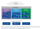
For high-performance applications, system architects have incorporated a stack of memory die in a 2.5D package configuration with a processor chip – see the figures below for a typical implementation, and expanded cross-section. These high-bandwidth memory (HBM) architectures typically employ four (HBM, 1st gen) or eight (HBM2/2E) DRAM die attached to a “base” memory controller die. The stack utilizes microbumps between die, with through-silicon vias (TSV’s) for the vertical connections.
A silicon interposer with multiple redistribution metal layers (RDL) and integrated trench decoupling capacitors supports this 2.5D topology, providing both signal connectivity and the power distribution network to the die.
A more recent package innovation provides the capability to attach two heterogeneous die in a 3D configuration, in either face-to-face or face-to-back orientations (with TSV’s). This capability was enabled by the transition of (dense) thermo-compression bonding for die attach from R&D to production status.
Previous semiwiki articles have reviewed these packaging options in detail. [1, 2] Note that the potential for both these technologies to be used together – i.e., 3D heterogeneous die integration (“front-end”) with 2.5D system integration (“back-end”, typically with HBM) – will offer architects with a myriad of tradeoffs, in terms of: power, performance, yield, cost, area, volume, pin count/density, thermal behavior, and reliability. A new EDA tools/flows discipline is emerging, to assist product developers with these tradeoffs – pathfinding. (Look for more semiwiki articles in this area in the future.)
Thermo-compression Bonding for HBM’s
The high-performance applications for which an integrated (general-purpose or application-specific) processor and HBM are growing rapidly, and they need an increasing amount of (local) memory capacity and bandwidth. To date, a main R&D focus has been to expand the 2.5D substrate area, to accommodate more HBM stacks. For example, TSMC has recently announced an increase in the maximum substrate area for their 2.5D Chip-on-Wafer-on-Substrate (CoWoS) offering, to enable the extent of the interposer to exceed 1X the maximum lithographic reticle size. RDL connections are contiguous across multiple interposer-as-wafer exposures.
Rather than continuing to push these lateral dimensions for more HBM stacks, there is a concurrent effort to increase the number of individual memory die in each stack. Yet, the microbump standoffs with the TSV attach technology introduce additional RLC signal losses up the stack, with a less-than-optimum thermal profile, as well.
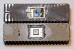
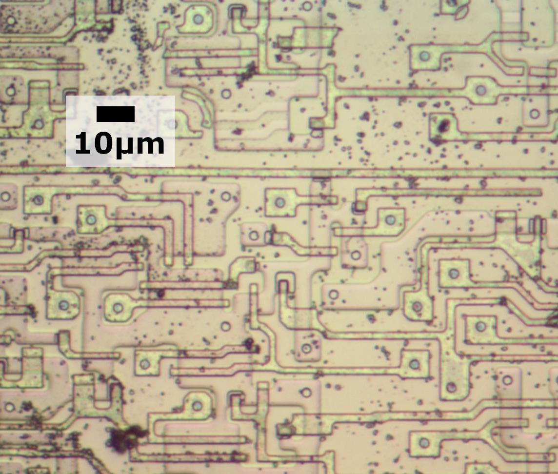
At the recent VLSI 2020 Symposium, TSMC presented their data for the application of thermo-compression bonding used in current 3D topologies directly to the assembly of the HBM stack – see the figure below. [3]
A compatibility requirement was to maintain a low-temperature bonding process similar to the microbump attach method. Replacing the microbumps between die with thermo-compression bonds will result in reduced RLC losses, greater signal bandwidth, and less dissipated energy per bit. The simulation analysis results from TSMC are shown below, using electrical models for the microbumps, compression bonds, and TSV’s. Note that TSMC pushed the HBM configuration to 12-die and 16-die memory stacks, well beyond current production (microbump-based) designs.
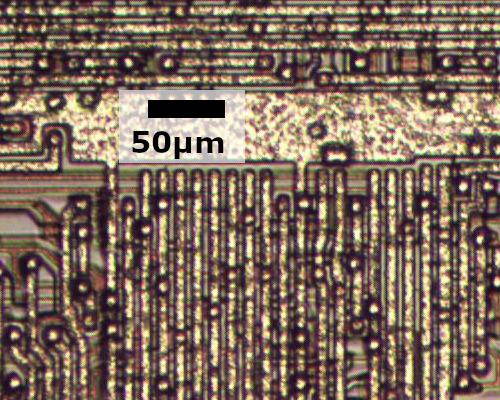
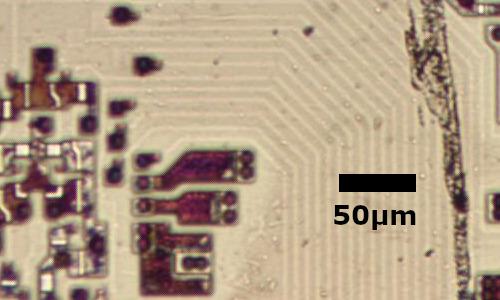
To demonstrate the manufacturability of a very tall stack with bonding, TSMC presented linear resistance data in (bond + TSV) chains up and down the die – see the figure below.
A unique characteristic of the bonded HBM stack compared to the microbump stack was the reduction in thermal resistance. The directly-attached dies provide a more efficient thermal path than the die separated by the microbumps. The TSMC data is shown below, illustrating the improvement in the temperature delta between HBM stack and the top (ambient) environment.
The conclusion of the TSMC presentation offered future roadmap opportunities:
- Tighter thermo-compression bond pitch (< 10um) is achievable, offering higher die-connections/mm**2. (Bandwidth = I/O_count * data rate)
- Additional R&D investment is made to pursue increased thinning of the DRAM die, further reducing the RLC insertion losses, improving the thermal resistance (and allowing more die in the same package volume). For example, the current ~60um die thickness after back-side grinding and polishing could be pushed to perhaps ~50um.
The figure on the left below highlights the future targets for bond connection density, while the figure on the right shows the additional bandwidth and energy/bit improvements achievable with a more aggressive HBM memory die thickness.
The application of 3D packaging technology thermo-compression bonding to HBM construction will enable greater memory capacity and bandwidth, required by high-performance computing applications. System architects now have yet another variable to optimize in their pathfinding efforts.
For more information on the 2.5D and 3D heterogeneous packaging technology offerings from TSMC, please follow this link.
-chipguy
References
[1] https://semiwiki.com/semiconductor-manufacturers/tsmc/285129-tsmcs-advanced-ic-packaging-solutions/
[2] https://semiwiki.com/semiconductor-manufacturers/tsmc/8150-tsmc-technology-symposium-review-part-ii/
[3] Tsai, C.H., et al., “Low Temperature SoIC Bonding and Stacking Technology for 12/16-Hi High Bandwidth Memory (HBM)”, VLSI 2020 Symposium, Paper TH1.1.
Images supplied by the VLSI Symposium on Technology & Circuits 2020.


