RVN! 26 Banner revised (800 x 100 px) (600 x 100 px)

Embedded Systems Development Flow

Embedded Systems Development Flow
by Daniel Nenni on 11-09-2020 at 6:00 am

Webinar SoC 1

Earlier this year. as part of my coverage of the virtual Design Automation Conference (DAC), I interviewed Agnisys CEO and founder Anupam Bakshi. He talked about the new products they introduced at the show and filled me in on the history of the company and his own background. Recently, Anupam presented the webinar “System Development Using Agnisys” and I was curious about their status so I checked it out.

My main impression is that the company has done a nice job of moving beyond focusing on individual products to show how they can be used together in chip development. I think that’s important for two reasons. First, Agnisys has quite a few products for a relatively small company. I count eight products or product families, with some variations. For example, their flagship IDesignSpec™ (IDS) is available as a Microsoft Word plug-in, a Microsoft Excel plug-in, a batch tool, or their new IDS NextGen GUI and executable specification editor. For users looking to solve a specific design or verification problem, it seems clear from their website what product to choose.

It’s also important to show users how Agnisys tools fit together in a flow to contribute to the overall design and verification effort, and I was pleased to see that the recent webinar addressed exactly that topic. The focus was on the design and verification of embedded systems, which is a broad topic. Anupam noted that the system-on-chip (SoC) hardware design can use ASIC or FPGA technology and include a wide range of IP from internal teams, commercial providers, and open-source projects. The software components include firmware and device drivers that interact closely with the hardware and extend up to the operating system and applications. I was impressed that the company covers so much of the embedded hardware-software spectrum.

The webinar then discussed some of the design and verification challenges for SoC development, identifying specification changes as a major problem. That seems accurate to me. Every time that the architecture spec is updated, it has ripple effects to the hardware design and, quite often, requires software updates as well. Both the hardware and software must be re-verified to test the changed functionality and ensure that nothing was broken by the updates. Then the entire system must be validated, consuming expensive resources and delaying tapeout. These issues are bad enough, but it’s even worse when the teams get out of sync. This is hard to avoid when the spec changes are communicated to the engineering groups at different times and implemented on different schedules.

It seems to me that automating the design and verification process from executable specifications is the key to the Agnisys solution. Their tools generate RTL design code, verification testbenches and tests, device drivers, documentation, and even programs that can be used to test the fabricated chips. Obviously, this saves a lot of time and money, but it also ensures that all development teams remain in sync. Specification changes are propagated immediately to all stakeholders with the simple push of a button in the GUI or a simple command in batch mode. Agnisys automates the design and verification of registers, memories, sequences, bus interfaces, and several types of IP. They also provide tools to connect all these elements, plus user-developed blocks, into a complete SoC.

What I liked best about the webinar is that it wasn’t a pitch for Agnisys products, full of features and benefits. Instead, the team put together a small but realistic SoC design and walked us through the process of using Agnisys tools within an embedded systems development flow. The design averages sensor data received over an I2C interface. Sensor values are read in and converted into an averaged value by user application logic, all under control of software running on a CPU. Anupam showed the input specification formats and the different types of code automatically generated at each stage of the process. I appreciated seeing these technical details rather than just a bunch of sales slides, although I wish that they also showed some of the tools running.

I’d like to thank Agnisys for alerting me to this webinar and for putting together quite an interesting event. If you missed it you can register to watch the recorded version here. I hope that you find it as interesting as I did.

Also read:

Automatic Generation of SoC Verification Testbench and Tests

Register Automation for a DDR PHY Design

CEO Interview: Anupam Bakshi of Agnisys


The Future of FPGAs

The Future of FPGAs
by Kris Kachris on 11-08-2020 at 10:00 am

The Future of FPGAs

On June 1, 2015 Intel and Altera announced , that they had entered into a definitive agreement under which Intel would acquire Altera for $16.7 billions. That was a major milestone for the FPGA community as Xilinx and Altera were the main FPGA vendors.

After the official announcement of AMD to acquire Xilinx, there is a huge concern on the FPGA community on the future of FPGAs.

The main goal of the Xilinx acquisition is to create the industry’s leading high performance computing company, “significantly expanding the breadth of AMD’s product portfolio and customer set across diverse growth markets where Xilinx is an established leader” according to AMD. But what is the main market that Xilinx is leading?


Alveo, VERSAL and Vitis AI

Xilinx released 3 years ago a powerful FPGA platform named Alveo. Alveo was the first FPGA board developed originally by Xilinx to serve as an Accelerator card to compete with GPUs. Until then, Xilinx was mostly developing the FPGA chips and was depending on other vendors for the FPGA cards. With the advent of the Alveo cards (and most recently Versal) Xilinx wanted to offer a powerful platform under it’s brand name to serve as an accelerator card. Xilinx developed very fast an impressive ecosystem around the Alveo platform including several companies that were utilizing the power of Alveo cards to accelerate several applications in the domain of machine learning, deep neural networks, databases, Natural Language Processing, Genomics, and quantitative finance. The main goal of the Alveo cards was to provide a powerful alternative to GPUs for deep learning.

Xilinx also offered an integrated EDA tool (SDAccel then Vitis) that allowed the programming of FPGAs from high-level programming languages like OpenCL and C/C++ without the need to use VHDL or Verilog. These tools allowed software developers without prior knowledge of FPGAs to be able to develop their own accelerators (although a deep understanding of the FPGA technology is required to develop efficient hardware accelerators using OpenCL).

NVIDIA, ARM and Mellanox

Almost one month ago, Nvidia announced the intention to acquire ARM for $40 Billion, “creating world’s premier computing company for the age of AI”. One of the reason of the acquisition was to allow Nvidia’s goal to develop the Data Processing Units (DPU) that consist of:

  • software programmable, multi-core CPU (aka ARM)
  • high-performance network interface (aka SmartNIC) (aka Mellanox)
  • rich set of flexible and programmable acceleration engines (aka Nvidia GPUs)

So after the acquisition of Xilinx from AMD, what will be the future of FPGAs.

Intel has a rich portfolio of hardware accelerators including powerful Xeon processor, GPUs, FPGAs and ASIC for deep learning. So what is the main market that FPGA are targeting at Intel? In one of the Intel presentations it was shown that Intel aim to utilize FPGAs in 3 specific markets:

  • Natural Language Processing (BERT)
  • Fraud Detection (LSTM)
  • Smart Cities (Inference).

So it seems that Intel is mainly focused on applications where low latency is critical and FPGAs can provide lower latency compared to other platforms. However it still remains to see how these FPGA targeting deep learning applications will differentiate from the ASIC deep learning platforms such as the one based on Habana Labs. Intel acquired Habana labs, for $2 billion for their technology on high performance deep learning inference and training.

The future of FPGAs

After the relevant acquisitions I think it is clear to everyone that we are moving on the era of Heterogeneous Data Processing Platforms where computing platform will include SmartNICs, multi-core processors and hardware accelerators and the user will have to select a complete solution instead of mix-and-match. Intel, AMD and Nvidia will offer complete computing platforms with their own proprietary accelerators and SmartNICs.

The benefits could be easier deployment and better integration but the option to select the best of each world will not be feasible any more or at least it will be more challenging (e.g. a selection of FPGA from Xilinx, Intel Xeon Processor and a GPU from Nvidia).

For Intel and AMD it will be hard to promote FPGAs in the domain of deep learning, for example, while other platforms will be available under their own brand name. Maybe FPGAs will mostly be utilized in their bread-and-butter market (networking and telecom like vRAN and 5G) while other platforms (GPUs, ASICs) will be promoted for deep learning.

The main benefit of FPGAs is the programmability to support tailored-made architectures. This means that they can adapt much faster to new algorithms or applications. This competitive advantage is of paramount importance especially in the domain of deep learning where new models are developed by ML engineers and data scientists. FPGAs can be programmed with the new tailored-made model/algorithm and can provide better performance compared to other platforms. Especially in application that bit-level processing is required, like packet processing, genomics and bitcoin mining, FPGAs has shown much better performance than other platforms. In deep learning applications, FPGAs can provide lower latency and high performance especially when reduced number of bits are used. (e.g. Xilinx FINN). So it seems that FPGAs can have a major role in the new processing ecosystem and not be used only for the SmartNIC applications.

In any case, in order to make FPGAs attractive as an accelerator platform, we need also to provide the required framework that will allow easy and scalable FPGA deployment. That is why a vendor-agnostic framework is required that allows to deploy FPGAs as easy as GPUs or CPUs.

In the domain of embedded system, FPGAs can still prevail. Both Xilinx and Intel provide SoC-based FPGAs with ARM cores that are widely used for embedded applications. Nvidia has stated that will still allow the use of ARM cores by 3rd parties so Xilinx and Intel will keep using ARM in their SoC-based FPGA (until they switch to RISC-V processors maybe in a couple of years).

The FPGA community is quite large and is keep growing. Several conference like FCCM, FPGA and FPL show that there is a large community supporting and promoting the use of FPGAs. However, it still remain to be seen if FPGAs will continue to serve as general-purpose accelerators or their applications will be much more limited in networking and telecom applications.


Intel’s Secret Key to Decrypt Microcode Patches is Exposed

Intel’s Secret Key to Decrypt Microcode Patches is Exposed
by Matthew Rosenquist on 11-07-2020 at 8:00 am

Intels Secret Key to Decrypt Microcode Patches is Exposed

A group of security vulnerability researchers, after many months of work, were able to figure out the update process and secret key used to decrypt Intel microcode updates for the Goldmont architecture product lines.

This is an important finding as it peels back yet another layer of the onion that protects the core CPU from malicious manipulations. It allows outsiders to pull back the veil that has obfuscated patch contents, crafted to close vulnerabilities in Intel CPU’s, so they may understand what is exploitable in the processor. This is a leap forward for hardware hackers. It is the next step that assists in dismantling the traditional defense structures that have protected the update process of Intel core CPUs.

The discovered key itself does not represent a direct system hacking threat at the moment, but it will provide researchers a much greater level of access and visibility to the inner workings of the CPU and may likely facilitate the discovery of many other vulnerabilities.

The extracted RC4 secret key employs a symmetric cipher that has known weaknesses dating back to 2001 and has not been considered secure for most usages since 2015.  This key handless both the encryption and decryption of data. From all accounts, it appears the signing key, which verifies the legitimacy of a patch, was not compromised. Therefore, it would be difficult to remotely push a maliciously crafted microcode update to systems, as the devices should disregard it because it lacks the necessary authentication.

However, given the access to the key and onboard debug service mode, there may be a possibility that an attacker with direct physical access to the system might be able to run locally modified instructions on a targeted system. There would be limitations but the access and control would potentially be unprecedented. Overall, the greater threat is how this capability will enable the next steps of vulnerability research which could open up much greater avenues of attack.

Dan Goodin, Security Editor at Ars Technica, reached out to Intel for their position, which he published in his outstanding article. The official response from Intel reads like it was written by lawyers and engineers, but absent cybersecurity mindsets. It talks only about the current exposure and not the long-term likely ramifications.

“The issue described does not represent security exposure to customers, and we do not rely on obfuscation of information behind red unlock as a security measure. In addition to the INTEL-SA-00086 mitigation, OEMs following Intel’s manufacturing guidance have mitigated the OEM specific unlock capabilities required for this research. The private key used to authenticate microcode does not reside in the silicon, and an attacker cannot load an unauthenticated patch on a remote system.”

Intel should be worried. The flood of vulnerabilities and exploits in recent months against their products has shown systemic problems. The focus and research against hardware is only increasing and Intel is a prime target. The exposure of the microcode key will help accelerate the discovery of more secrets that pose a risk to the security of Intel’s products.

If you like these updates, click the Like button and be sure to subscribe to the Cybersecurity Insights channel for more rants, news, and perspectives.


What the Hell is C-V2X and Should I Care?

What the Hell is C-V2X and Should I Care?
by Roger C. Lanctot on 11-07-2020 at 6:00 am

What the Hell is C V2X Should I Care

Automotive innovations have the greatest impact when they create what can only be described as magical experiences. The most magical experience of all is the car that avoids hitting things, or the car that parks itself.

I feel pretty strongly that cars should not hit things – that this is a product defect. The introduction of C-V2X cellular technology – as part of the onset of LTE Advanced network systems and, later, 5G – will bring enhanced situational awareness and collision avoidance to cars as soon as next year.

Generally, consumers have failed to warmly embrace wireless connectivity – especially where auto makers want to charge a monthly or annual subscription. C-V2X technology delivers its value proposition without that subscription – which makes it even more magical.

Later today, the 5GAA (5G Automotive Association) is hosting a virtual showroom where a variety of C-V2X-based functions will be demonstrated including avoiding vulnerable road users, anticipating traffic light phase changes, and enabling remote vehicle control. The most important reality behind these enhanced capabilities is that they will become immediately available to consumers who purchase vehicles so equipped, but they also lay the groundwork for an ever increasing array of functionality long after their initial deployment.

Perhaps even more important is the fact that these enhanced features and functions are being brought to market through the collaboration of car companies, wireless carriers, infrastructure providers, Tier 1 hardware and software providers, and local departments of transportation – all of whom will be represented as part of the 5GAA C-V2X showroom event today. And, finally, the life saving communications enabled by C-V2X – created by an interface providing for direct device-to-device communications outside of the wireless network – will function whether the cellular device is provisioned or connected to a network or not.

The onset and deployment of C-V2X technology will change the way consumers think about vehicle connectivity and has the potential to arrest the inexorable rise in highway fatalities. I will be hosting the 5GAA event and the organization welcomes all interested parties to attend.

About 5GAA
The 5G Automotive Association(5GAA) is a global, cross-industry organisation of companies from the automotive, technology, and telecommunications industries (ICT), working together to develop end-to-end solutions for future mobility and transportation services.

Created on September 2016, the 5GAA unites a large member base, including 8 founding members: AUDI AG, BMW Group, Daimler AG, Ericsson, Huawei, Intel, Nokia, and Qualcomm Incorporated.

Since its inception, 5GAA has rapidly expanded to include key players with a global footprint in the automotive, technology and telecommunications industries. This includes automotive manufacturers, tier-1 suppliers, chipset/communication system providers, mobile operators and infrastructure vendors. More than 130 companies have now joined 5GAA.

Diverse both in terms of geography and expertise, 5GAA’s members are committed to helping define and develop the next generation of connected mobility and automated vehicle solutions.


AMD and Intel Update with Xilinx

AMD and Intel Update with Xilinx
by Daniel Nenni on 11-06-2020 at 10:00 am

AMD Xilinx Acquisition

The AMD acquisition of Xilinx is certainly big news but as an insider looking at the media coverage I think there are a few more points to consider. While most of the coverage has been positive there will always be negatives and we can look at that as well.

Intel acquired Altera in 2015 for $16.7B at a 50% premium which was a major disruption for the FPGA industry. Altera and Xilinx were in a heated battle for manufacturing supremacy when Xilinx joined Altera at TSMC for 28nm and beat Altera to first Silicon. Altera responded by moving manufacturing to Intel at 14nm which resulted in Intel acquiring Altera. Looking back, it was a great move which provided Intel with a larger cloud footprint. Rumors of a Xilinx acquisition swirled afterwards but a 50%+ price premium was expected and the motivation on either side was not strong enough.

AMD and Intel are also in a heated battle for manufacturing supremacy. With AMD’s move to TSMC at 7nm the battle has shifted in AMD’s favor. Based on the latest investor calls AMD is in a very strong position against Intel for 7nm and 5nm products. Xilinx also reported a great quarter with beats at the top and bottom line with the Data Center Group hitting record revenue, up 23% Q/Q and logging 30% annual growth. This is another one of those 1+1=3 acquisitions.

And for those naysayers who think AMD will abandon the mainstream FPGA market there really is a simple solution: Keep Xilinx as a separate business unit, FPGA business as usual but also as a leverage for AMD chip business and vise versa.

The other negative I heard is that AMD and Xilinx will be fighting for leading edge wafers which is not true. Xilinx designs leading edge products but it takes time for Xilinx customers to get systems developed, qualified and shipped in volumes. Xilinx stayed on 28nm for the longest time and the new Xilinx Vertex Ultrascale+ products utilize 14/16nm process technology.

From the CEOs:

“Our acquisition of Xilinx marks the next leg in our journey to establish AMD as the industry’s high performance computing leader and partner of choice for the largest and most important technology companies in the world,” says AMD President and CEO Dr. Lisa Su in a press release.

“This is truly a compelling combination that will create significant value for all stakeholders, including AMD and Xilinx shareholders who will benefit from the future growth and upside potential of the combined company. The Xilinx team is one of the strongest in the industry and we are thrilled to welcome them to the AMD family.”

“We are excited to join the AMD family. Our shared cultures of innovation, excellence and collaboration make this an ideal combination. Together, we will lead the new era of high performance and adaptive computing,” adds Victor Peng, Xilinx president and CEO.

“Our leading FPGAs, Adaptive SoCs, accelerator and SmartNIC solutions enable innovation from the cloud, to the edge and end devices. We empower our customers to deploy differentiated platforms to market faster, and with optimal efficiency and performance. Joining together with AMD will help accelerate growth in our data center business and enable us to pursue a broader customer base across more markets.”

Sounds good to me. Now let’s talk about the other insider synergies. First and foremost is the Xilinx – TSMC relationship. The Xilinx foundry group is one of the best I have seen. I’m not saying AMD has a bad foundry group, but Xilinx has been with TSMC since 28nm and has been first to silicon on each and every node since. There is only upside for AMD here. And this includes packaging. Remember, Xilinx is a close packaging partner with TSMC (CoWoS).

Another interesting synergy is company culture. Since the beginning of AMD their marketing has outpaced engineering. Blame Jerry Sanders (AMD’s founding CEO and showman extraordinaire).  Thankfully, Lisa Su embraced that culture and brought products to market that now more evenly pace marketing.

With Xilinx, on the other hand, engineering always outpaced marketing. We included a chapter on the history of Xilinx in our first book “Fabless: The Transformation of the Semiconductor Industry” as they were one of the first fabless companies. This engineering centric culture is a biproduct of highly technical CEOs of course.

If Lisa Su is able to combine the two cultures it will be a big part of the 1+1=3 acquisition equation for sure.

Another interesting question, what is next for the FPGA industry? Programmability has never been a more critical part of the semiconductor industry as a whole. In my opinion another acquisition is looming. No, not Lattice semiconductor or Microchip. I see Achronix as being the next hot FPGA property and hopefully Nvidia has enough money left after acquiring Arm. Achronix is a $200M or so 150+ person company that is located conveniently close to Nvidia. If you combine their speedy high capacity FPGAs with the Nvidia AI/HPC software ecosystem it will be a 1+1=300 acquisition, absolutely.


Leading Edge Foundry Wafer Prices

Leading Edge Foundry Wafer Prices
by Scotten Jones on 11-06-2020 at 6:00 am

Slide1

I have seen several articles recently discussing foundry wafer selling prices for leading edge wafers, these articles all quote estimates from a paper by the Center for Security and Emerging Technology (CSET). The paper is available here.

My company IC Knowledge LLC is the world leader in cost and price modeling of semiconductors and MEMS. We have been selling commercial cost and price models for over twenty years and our customer base is a who’s who of system companies, fabless, foundries and IDMs, OEMS, materials companies and analysts. I thought it would be interesting to examine how the estimates in the paper were produced and how realistic they are.

Capital Costs

CSET begins their analysis looking at TSMC’s financial releases and find from 2004 to 2018 that revenue can be broken down into 24.93% depreciation, 36.16% other costs and 35.91% operating profit. They also come up with a 25.29% capital depreciation rate. They then go on to calculate capital consumed per wafer and then use these percentages to infer other costs. I see a couple of problems with this approach, one, it assumes these ratios are the same for all nodes, they aren’t, and two, the depreciation rate makes no sense as I will explore further below.

The capital consumed calculation is as follows:

“To obtain capital consumed per wafer, we first calculate capital investment per wafer processed per year. TSMC currently operates three GigaFabs (Fabs 12, 14, and 15) with a fourth (Fab 18) scheduled to come online in 2020 with expansion thereafter.”

This ignores TSMC’s Fab 16 with two phases in China.

“These four fabs include a total of 23 fab locations each with a known initial capital investment in 2020 USD— representing investments in facilities, clean rooms, and purchase of SME—and annual 300 mm wafer processing capacity.”

Fabs 12, 14 and 15 are each 7 phases, Fab 18 is planned to be 6 phases, apparently they are considering the 21 phases from Fabs 12, 14, and 15 plus 2 phases from Fab 18 that have recently come on-line and ignoring Fab 16 (although Fab 16 is relatively small and therefore less significant than the GigaFabs).

They plot capital investment per 300mm wafer processed per year and fit an exponential trend line to the plot.

I do not know what their specific data source is, TSMC sometimes announces fab capacity and initial investment but not always and these are often more aspirational numbers than actual costs. These fabs also often have an initial cleanroom build and then are equipped over time as they are ramped up with ramps covering more than one year. The ultimate fab capacity is often the result of additional investments. It is not clear to me how this becomes a cost per wafer per year with this approach. These values eventually get converted to capital investment per wafer per year by node based on the year and quarter each node was introduced and then assuming the capital investment per wafer by year represents that node. The problem is TSMC is not always only ramping one node in any given year plus the other issues discussed above.

The way we address capital cost in our models is fundamentally different and more detailed.

  1. For each node we built a representative process flow, this is done based on our own experience, consultation with industry experts, conference papers, patents, and actual construction analysis from our strategic partner TechInsights.
  2. We maintain a database of every 300mm wafer fab in the world tracking the initial and all upgrade states. This database is a combination of public and private sources.
  3. We maintain a database of equipment throughput, cost and footprint by node and wafer size. Once again this is based on public and private sources. Our Strategic Cost and Price Model is in use at all the major equipment OEMs and we have an extensive network of sources for this information.
  4. For each 300mm fab we calculate a fab size and cost and equipment set based on the specifics of the process, and the fab states. We calculate this for the initial fab state and up to twelve upgrades or expansions per fab.

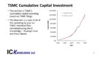
With the amount of information going into these calculations and the complex methods used we need to validate our methods. Around 2000 – 300mm fab began to come on-line and quickly accounted for most of the capital spending at all the major semiconductor companies. For TSMC as an example, we have taken their publicly disclosed capital spending each year since 2000 and plotted it versus year as a cumulative number. We have then modeled all their 300mm fabs and spending by fab by year and added that up to create a cumulative plot. After accounting for some residual 200mm spending in the early years and any spending not yet on-line (our spending calculations are based on on-line dates) we get the following plot.

Figure 1. TSMC calculated versus actual cumulative capital spending.

 The resulting plot shows excellent match. We have done this same analysis for Samsung, Intel, Micron Technology and many others with equally good correlation.

TSMC typically focuses a fab on a single node so we now have capital costs per wafer-out estimates by node. Comparing our estimates by node to the estimates in row 2 of table 9 in the CSET paper we find that at the 90nm node the values are similar, but they steadily diverge as the nodes get smaller.

In the CSET paper rows 3 and 4 provide a net capital depreciated and undepreciated capital at the start of 2020 that are then used with a 25.29% depreciation rate to get the capital consumed per wafer value presented in row 5. This whole calculation makes no sense to me. TSMC has disclosed they use 5-year straight-line depreciation for equipment and 10-year straight-line for facilities. What this means is that if you put a piece of equipment on-line you write-off 20% of the equipment investment each year for the first 5 years and then the depreciation goes to zero in year 6. For facilities you write-off 10% of the value each year for 10 years and then the depreciation goes to zero. 90nm in 2020 is fully depreciated and even brand new 5nm investment is only depreciating at something less than 20% after blending equipment and facility depreciation.

Applying five-year straight-line for equipment, equipment installation and automation and ten-year straight-line depreciation to facilities values from our calculation we get the following depreciation by node plot. Also, on the plot is TSMC’s reported depreciation and as in the previous figure you can see the match is excellent.

Figure 2. TSMC calculated depreciation by node and quarter versus TSMC reported depreciation.

Based on these plots and other comparisons we have made it is clear our capital calculations are highly accurate.

Other Costs and Markup

This bring us to the other elements that add up to revenue.

First, to complete the wafer cost calculation:

  1. Starting Wafer – starting wafers are purchased from wafer suppliers and we have contacts at wafer brokers and wafer suppliers who provide us with the open market pricing.
  2. Labor – we have an extensive database of direct and indirect labor rates by country and year built up from a network of private and public sources.
  3. Equipment maintenance – we use a percentage of the capital investment in equipment to estimate the equipment maintenance cost. The percentage varies depending on wafer size and product type being made in the fab, for example memory is different than logic.
  4. Facilities – we do detailed facilities operating cost calculation accounting for electric and natural gas rates by country and year and equipment requirements, ultrapure water cost, waste disposal, facilities maintenance, insurance costs, and more. Once again, we have public and private data sources.
  5. Consumables – based on the process flow we calculate the usage of hundreds of individual consumables and combing that with a database of cost by consumable and year calculate the total consumable costs. We get consumable usage and cost data from our strategic partner Linx Consulting as well as an extensive network of materials suppliers.

The summation of these values and the depreciation results in manufacturing costs per node.

To get to selling price, a gross margin must be applied where the gross margin includes Selling, General and Administrative Costs (SG&A), Research and Development Costs (R&D) and Operating Profit. TSMC discloses average gross margin in their filings, however gross margin is not flat across their product line (it also varies with fab utilization). When a new process comes on-line, depreciation costs are high but then as the equipment becomes fully depreciated the wafer manufacturing costs drops more than in-half. TSMC and other foundries typically do not pass all the cost reduction that occurs when equipment becomes fully depreciated on to the customer, the net result is that gross margins are lower for newer processes and higher for older fully depreciated processes. We account for this in our calculation, but once again the calculation disclosed in CSET the paper assumes the other wafer costs and gross margin are consistent from node to node.

In our case we have a variety of ways to check our wafer prices including customers who buy wafers and compare them to our calculations, and our ability to use proprietary methods to compare our results to company filings. For example, we have compared our calculated results to TSMC’s filings every quarter from Q1-2000 to Q2-2020 with excellent match every quarter.

This brings us to the key question, how accurate are the row 7 “Foundry sale price per wafer” values in the paper and the answer is not very. There is basically an error slope to the results with the 90nm prices being too low and at 5nm the prices are too high.

Conclusion

Although the value in the CSET are not off by an order of magnitude, they are off. I have customers frequently ask me for rules of thumb and I tell them my rule of thumb is that all rules of thumb are wrong.  Accurate estimates of wafer manufacturing costs and selling prices require detailed calculations such as are embodied in our commercial cost and price models. We currently offer five cost and price models targeting different segments of the semiconductor and MEMS industries.

For more information on our models please go to www.icknowledge.com

Also Read:

VLSI Symposium 2020 – Imec Monolithic CFET

SEMICON West – Applied Materials Selective Gap Fill Announcement

Imec Technology Forum and ASML


Creating Workflows for HCL Compass Just Got Easier

Creating Workflows for HCL Compass Just Got Easier
by Mike Gianfagna on 11-05-2020 at 10:00 am

Creating Workflows for HCL Compass Just Got Easier

Workflows allow the world to function. The orderly process of sequencing tasks and automating handoffs creates tremendous potential for efficiency and error avoidance. As they say, time is money and workflows can save a lot of time. The principle applies in all kinds of industries. If you design chips for a living, you’re very familiar with the standard design flow you and your team uses.  The software versions, the technology files, the scripts and the supporting data form the fabric of your work environment. In the DevOps world, it’s the same. The tools used and the resources managed may be different, but the end goal is the same. In this DevOps environment a recent enhancement to HCL Compass caught my eye. Let’s explore how creating workflows for HCL Compass just got easier.

In August, I discussed HCL’s Compass and its ability to deliver defect tracking and more. The tool is actually quite broad in its application Beyond issue tracking, it provides the ability to integrate typically disparate functions such as analysis, development, testing, and deployment. This integration provides good notifications to keep the team in sync which also improves collaboration. HCL describes full lifecycle traceability with such a workflow. In their words:

Customize and enforce consistent development processes and achieve an integrated, consolidated view across the project. In addition to process automation and lifecycle traceability, security features such as user authentication, user authorization, electronic signatures, and audit trails are critical to helping ensure compliance with internal and external requirements.

These are all significant benefits but achieving them requires another very important ingredient. Customization. No one workflow fits all scenarios and scaling to the enterprise level makes customization even more important. In fact, you will see the this at the very top of the HCL Compass web page:

Flexibility Through Customization

Customization requires interaction with the product through an applications programming interface (API). This is why a recent announcement from HCL caught my attention:

Unlock new possibilities for managing workflows with HCL Compass’s REST APIs

Some definitions are in order. Prior to this announcement, the Perl API or Java Native Interface were available for interaction with HCL Compass at a programming level. One could call these interfaces a bit heavy, requiring domain-specific knowledge and a fair amount of time to achieve a desired result.

With the release of version 1.0.1 of Compass, a suite of REST APIs become available that enable lots of new capabilities. For those who not familiar with the term, REST stands for representational state transfer. A REST API defines a set of constraints that are used to create web services. To prove the inventors of this technique have a sense of humor, web services that conform to the REST style are called RESTful web services, providing interoperability between host systems and the internet. In general, a REST API will provide a lot of flexibility with a structure that is predictable and easy to use. If you’d like to learn more, you can access a REST API tutorial here.

Back to version 1.0.1 of Compass. The new REST API allows easy implementation of tasks such as viewing and modifying of records or executing complex queries. These are items that will be needed to build a custom workflow. A sample IOS application is included in the release. Integrating with a mobile device is a popular part of any enterprise deployment. Full source code and a detailed tutorial is available here. Custom workflows are an important ingredient for any enterprise application deployment. HCL seems to have a well thought out strategy to support Compass custom workflow development. Indeed, creating workflows for HCL Compass just got easier.


Verification IP for Systems? It’s Not What You Think.

Verification IP for Systems? It’s Not What You Think.
by Bernard Murphy on 11-05-2020 at 6:00 am

System VIP2 min

When I think of verification IP (VIP), I think of something closely tied to a protocol standard – AMBA, MIPI or DDR for example. Something that will generate traffic and run protocol compliance checks, to verify correct operation of an IP or as a model to use in SoC verification. What would a VIP for systems be? Systems support multiple protocol interfaces. And they generate traffic and require checks that depend as much on the purpose of the SoC as on those interfaces. Moshik Rubin, a PM group director at Cadence helped me reinterpret the VIP concept for systems.

A superstructure for SoC verification

The goal is not to check a specific function but to provide a front-to-back superstructure for SoC-specific verification tasks, from test assembly and traffic generation to performance analysis and score boarding. This complements rather than replaces your existing verification investment (UVM libraries, etc). It looks conceptually familiar to existing verification components: test-bench assembly and VIP, PSS test generation, performance analyzer and score boarding. However, Moshik says they redesigned these from the ground up for the needs of modern heterogenous SoCs.

The purpose is to simplify stressing the system, to provide more automation for a very complex task. You want to ensure for example that you full stress the interconnect, maximizing load. That you fully load from the PCIe interface and you cover all the memory subsystem corner cases. The system maintains cache coherence across many masters, some with native CHI interface, some with legacy ACE interfaces from 3rd party suppliers. That data integrity is maintained across chip networks as packets are sliced and diced in the middle and reassembled later. And that you can flip these analyses back and forth between software-driven testing in emulation and FPGA prototyping and simulation as needed.

Assembly, traffic libraries reinvented

You were able to do some of this before for Arm-based designs, more exactly designs using Arm cores and interconnect fabrics. Now the solution works with any interconnect fabrics, including a mix – Arm NICs and coherent fabrics, NoCs, coherent NoCs and meshes, along with complex cache and memory architectures. And the design no longer has to be Arm-centric. It can be based on RISC-V or x86. Testbench assembly can start, as before, with an IP-XACT or CSV description. Build your own descriptions in Excel, parametrize them with Visual Basic if you are up for that. (Try it. It can be fun!)

Traffic is described through PSS, for which System VIP provides a predefined set for cache coherency, performance, PCIe and others. I asked Moshik about other traffic generators. He said they’ve provided built-in libraries where they see a lot of uniformity between customer needs. For other generators, such as Ethernet where they see a lot more variability, customers can easily add their own PSS models. Or use existing UVM components. Reinforcing that this is an overlay, not a replacement for your proven testbench infrastructure. All tests will generate for simulation, emulation or post-silicon, directed to either UVM or C++ generation.

Analysis and scoreboarding

The system performance analyzer equally has been redesigned to work with heterogenous designs (cores and on-chip networks). And to look at the whole SoC, not just the interconnect, so you can start with high-level views of performance bottlenecks and drill down anywhere. The system verification scoreboard also is IP-vendor agnostic. For example, now you can observe traffic in PCIe, CXL or DDR, check cache coherency, data coherency. These checks are no longer limited to interconnect boundaries.

A customer experience

Renesas presented on this topic at CadenceLIVE recently. The speaker commented that previously testbench creation, allocating and configuring active and passive VIPs could take weeks. Then generating test patterns with multiple masters driving competing threads could take a few days per test pattern. They saw improvements in efficiency of testbench creation and analysis very consistent with Cadence’s claim of up to 10X. If you watch the talk, this was just before the System VIP official release, which Moshik tells me is why the speaker still uses the old product names.

To learn more about Cadence System VIP, click HERE.

Also Read

How ML Enables Cadence Digital Tools to Deliver Better PPA

Clarity 3D Transient Solver Speeds Up EMI/EMC Certification

The Most Interesting CEO in Semiconductors!


What’s Driving This New Wave of Semiconductor Merger Mania?

What’s Driving This New Wave of Semiconductor Merger Mania?
by Wally Rhines on 11-04-2020 at 10:00 am

Predicting Semiconductor Business Trends SemiWiki

Nvidia/ARM $40B. AMD/Xilinx $35B. Marvell/Inphi $10B. Despite the disruption of COVID, a wave of high value semiconductor acquisitions is sweeping the industry. Why? Did something happen that stimulated this consolidation? Until 2015, the industry was experiencing continuous “de-consolidation” that started in 1965. Combined market share of the top 50 companies steadily decreased as small companies entered the market and grew to displace the previous leaders.

Predicting Semiconductor Business Trends After Moore’s Law

Even today, only one company, TI, has remained in the Top 10 since the 1950s. Growth prior to 2015 was largely organic rather than by acquisition. In 2015 and 2016, the consolidation generated by acquisitions of Broadcom, Freescale, Altera, Linear Technology and ARM provided a temporary burst in acquisition activity. Analog Devices’ July 2020 announcement of a proposed acquisition of Maxim, however, seems to have been a precursor to a new wave. Following are some possible differences in the industry today that might be driving this recent merger mania.

Cheap currency?
Market value for semiconductor stocks is volatile. Most acquisitions are done for a high percentage of cash, thus avoiding uncertainty of value and a lengthy shareholder approval process. In this case, the acquisitions are primarily for stock (over 60% for nVidia/ARM and Marvell/Inphi and 100% for AMD/Xilinx). AMD’s stock price has risen over 150% over the past year (2200% since Lisa Su took over in 2014) and now sells for a multiple of ten times revenue. nVidia’s stock is up 300% and now values the company at 25 times revenue, nearly two times the value of Intel despite having less than one sixth the revenue. Marvell is up 60% and sells at nine times revenue. When your currency is hot, maybe it is a good idea to convert it to something that has more lasting value, even if the company you acquire also has a high valuation compared to historical levels?

Market segment specialization?
One of the few semiconductor market segments that is destined to grow at a more rapid rate than the overall market for at least the next decade is the server market. All of these most recent announcements focus on growth of the cloud and the strength that these combinations will provide. For nVidia/ARM, it is a chance to take the next step toward challenging Intel’s dominance of the data center. Ditto for AMD/Xilinx. Even the Marvell/Inphi announcement focuses on “Marvell’s leadership in the cloud” while also highlighting 5G opportunities. Total server revenue increased 60% over the last four years and continues to be a standout in a year of relatively low semiconductor end equipment growth.

Regulatory approval?
Regulatory approval is a long and uncertain process. Uncertainty is the enemy of employee stability and customer loyalty. Companies usually don’t subject themselves to that uncertainty unless there’s a high likelihood of approval. The U.S. Federal Trade Commission has reasonably firm guidelines concerning the degree to which a combination may increase the market influence of a competitor. Frequently, the result depends upon what the FTC decides the relevant market is. In all these cases, there are larger competitors in both the total semiconductor market as well as relevant segments, except for graphics chips where the nVidia/ARM combination would have only a small effect upon the size of nVidia’s graphics chip strength. For European agencies, the controversial issue would likely be the threat of losing a local jewel rather than the actual market share effects. That kind of threat is usually handled by requiring future guarantees of employment or corporate location. MOFCOM in China is normally the most difficult and lengthy approval to achieve. In these recent cases, we are not dealing with a Qualcomm/NXP kind of transaction, where Chinese businesses lack power in dealing with one of the parties. MOFCOM gains little or nothing by veto of the transactions. Greater benefit can be achieved by making demands of the companies and the way they conduct business in China in the future.

Likelihood of successful integration?
Statistically, the larger the company being acquired, as a percent of the acquiring company’s revenue, the more difficult the integration. This is probably because of power and cultural struggles in the combined company after the merger. The most successful acquisitions occur when the acquiree retains a high degree of autonomy or when it is so small that it can readily change its culture to conform to the policies and management of the acquirer. At least in the cases of nVidia/ARM and AMD/Xilinx, the differences in their businesses argues for a high degree of autonomy after acquisition. In the nVidia/ARM case, there are restrictions that prevent tight integration so that disclosure of sensitive customer data can be prevented.

Economies of scale?
I leave this for last because it hasn’t been a primary driver for semiconductor acquisitions ever since silicon foundries became a major force in the industry. If companies buy their wafers from foundries, then the difference in wafer cost discount rate that results from growing company size through acquisition is too small to justify the transaction, unless the companies predominantly use their own manufacturing facilities, as in the case of some analog and RF companies. Increasingly, in recent times, semiconductor business cost differentiation comes from factors other than manufacturing, e.g. product definition, development and marketing costs, customer sales and support, administrative, legal, finance and regulatory costs, etc. The fact that all of these acquisitions are targeted at strengthening the companies in specific markets, like the cloud and AI, suggests that the companies see economies of scale in defining, designing, marketing and supporting products sold to similar customers in similar markets.

Maybe there’s nothing new driving these acquisitions?  Or maybe there are other forces of business viability that make combinations desirable right now?  Whatever the case, one may wonder if this merger mania puts us on a path to domination by a few big companies as has been the case in some other industries as they mature?

I doubt it. Whenever there is rapid change in technology, new companies enter an industry with innovative new products and gain market share from the incumbents. We are in a period of rapid semiconductor innovation.  After fifteen years of declining venture capital investment in chip companies, the annual investment has jumped to an average of more than $2 billion per year for the last three years and appears to be on track for $2B or more in 2020. Applications like AI, machine learning, 5G and the IoT are growing because of the increase in availability of big data and the need to analyze it, use it and protect it. The new companies and businesses that emerge will give the industry ample opportunity to create new leaders.


The Gold Standard for Electromagnetic Analysis

The Gold Standard for Electromagnetic Analysis
by Daniel Nenni on 11-04-2020 at 6:00 am

Example of a multi level board analyzed by HFSS

Ansys HFSS has been the world’s trusted gold standard for  electromagnetic analysis for many years. As chip designs get bigger and more complex many users report that they’re extremely happy with the gold standard accuracy of HFSS but wish it would run faster. Fortunately Ansys has introduced many capabilities to HFSS over the years that significantly speed up total turn-around time.

From matrix multi-processing delivered back in 1997, then parallel frequency points in 2005, onto a Distributed Memory Matrix solver in 2016, and enhanced GPU performance in 2020, HFSS has been delivering consistent speed and capacity improvements for over two decades. In addition to algorithmic improvements and better utilization of cluster computing, Ansys has also streamlined the process of HFSS simulation setup. Streamlined model import from layout automatically defines the excitations and bounding regions for the simulations.

Auto solution setup means the user simply defines the frequency range of interest, and then selects a slider bar setting of Speed, Balance, or Accuracy. The user may pick Speed for iteration and design exploration or Accuracy for validation and sign-off. From there Auto HPC takes over to optimally apply the total number of cores and/or machines available, and the solver is off and running. In addition, HFSS automatically distributes the adaptive solution across all the nodes, and then utilizes the same compute resources to distribute the frequency sweep.

However, some users have gotten stuck in the way they solve problems in HFSS. For example, one user designing 112 Gbps high-speed SERDES SoC packaging had been cutting down the design to solve only a quarter of the package. It was the same, now unnecessary, divide-and-conquer approach to electromagnetic solves they have been using for years. With a different solver, they  tried  to model the same subdivided structure. Utilizing just one quarter the number of cores HFSS 2020 solved the problem in half the time. With the solve time down to just an hour they decided to model the entire package in HFSS. To their surprise solving the entire package of 184 ports up to 50 GHz, took only 18 hours.

“We never expected to be able to sign-off a large package design like this in HFSS,” said the package design lead at a Silicon Valley based custom ASIC house specializing in high speed networking and communications. “We tried solving this larger structure in another recently released FEM- based solver but were never able to complete the analysis.”

Updates to Ansys HFSS over the years are re-defining the possibilities in scale and turnaround time for full-wave electromagnetic sign-off in today’s chip, package, and PCB design challenges.

For more information on how to speed up your HFSS simulations, be sure to check out the best practices  webinars. 

About Ansys

If you’ve ever seen a rocket launch, flown on an airplane, driven a car, used a computer, touched a mobile device, crossed a bridge or put on wearable technology, chances are you’ve used a product where Ansys software played a critical role in its creation. Ansys is the global leader in engineering simulation. Through our strategy of Pervasive Engineering Simulation, we help the world’s most innovative companies deliver radically better products to their customers. By offering the best and broadest portfolio of engineering simulation software, we help them solve the most complex design challenges and create products limited only by imagination. Founded in 1970, Ansys is headquartered south of Pittsburgh, Pennsylvania, U.S.A. Visit www.ansys.com for more information.

Also Read

Executive Interview: Vic Kulkarni of ANSYS

World’s Leading Chip Designers at IDEAS Digital Forum Show How to Streamline Design Flows and Reduce Design Cost

Ansys Multiphysics Platform Tackles Power Management ICs