RVN! 26 Banner revised (800 x 100 px) (600 x 100 px)

Podcast EP2: Moore’s Law, Dead or Alive?

Podcast EP2: Moore’s Law, Dead or Alive?
by Daniel Nenni on 01-08-2021 at 10:00 am

Dan and Mike are joined by Dr. Walden Rhines for a scenic tour of Moore’s Law. The genesis and evolution of Moore’s Law are discussed, along with the fundamental processes that have driven it. How the technology world continues to grow and innovate in spite of a slowing of Moore’s Law is a central theme of the discussion.

Wally Rhines is widely recognized as an expert in business value creation and technology for the semiconductor and electronic design automation (EDA) industries. https://en.wikipedia.org/wiki/Wally_Rhines

The views, thoughts, and opinions expressed in these podcasts belong solely to the speaker, and not to the speaker’s employer, organization, committee or any other group or individual.


IEDM 2020 – Imec Plenary talk

IEDM 2020 – Imec Plenary talk
by Scotten Jones on 01-08-2021 at 6:00 am

Imec Figure 1

On Monday morning at IEDM, Sri Samavedam of Imec opened the technical program with a plenary talk entitled “Future Logic Scaling: Towards Atomic Channels and Deconstructed Chips”. I am not generally a fan of plenary talks, I think the presenters often try to cover too much in their talks and end up not providing enough detail to be useful, but there was a lot of good content in this talk.

I asked Imec for the slides to include some of them in this article, but they declined to provide them although they did send me the paper. I find it strange that they will not provide the slides, the video presentation of the slides is on the IEDM web site for registered attendees to view and anyone with a screen capture utility can easily capture any or all the slides. I will make use of a couple of the figures from the paper to try to make up for the lack of the slides.

The first approximately seven minutes of the talk were justifying the need for continued development of leading-edge technology and some historical perspective, I am going to omit this part as I believe the average Semiwiki reader and IEDM participant understand this already.

EUV Patterning

The talk then jumped into an EUV patterning roadmap. The presenter stated he thought High-NA EUV will be available for path finding around 2023 and will need two to three years to be ready for production. This would result in High-NA EUV entering production in the 2025/2026 timeframe, significantly later than I would have expected.

The Imec roadmap is for 3nm logic nodes to have 44-48nm Contacted Poly Pitch (CPP) and 21-24nm Minimum Metal Pitches (MMP), the 2nm logic node to be 40-44nm CPP and 18-21nm MMP and the 1.5nm logic node to be 40-44nm CPP, and 18-21nm MMP. I expect TSMC to be make risk starts with a 3nm node in late 2021 and production in 2022 and the CPP and MMP to be in the range of the numbers Imec proposes. I expect TSMC’s 2nm node to make risk starts in 2023 and production in 2024 and once again to have CPP and MMP values in the range that Imec presented. For 1.5nm Imec does not show any reduction in CPP and MMP ranges presumably reflecting a change to stacked transistors (more on this later) as a technique to drive density.

The Imec roadmap shows the current 0.33NA EUV systems being used for 3nm and 2nm and High-NA (0.55NA) being introduced at the 1.5nm node, this is once again later than I expected. I have for some time expected High-NA EUV to miss the 3nm node (although others have discussed high-NA for 3nm), but I thought the systems would be available for 2nm. If High-NA EUV systems are not available until 1.5nm it would be strictly as a cost reduction technique since 1.5nm has the same pitches as 2nm, and 2nm would already have been in production. Several years ago, I gave a presentation to ASML and raised the idea that by the time High-NA EUV was available transistor stacking (CFETs) might make it irrelevant. While it is likely that High-NA EUV can provide a cost reduction versus multi-patterning with EUV, if this timeline is correct it will not be a technology enabler.

I reached out to ASML for a comment on this and got the following reply:

“We are aligning with customers on roadmap timing of High NA insertion in volume production, currently estimated to be in the 2025-2026 timeframe. We will work with them to ramp to HVM as quickly as possible. Looking back at prior transitions, like ArFi, usually it takes a couple of years to ramp to HVM after first tool shipments. So a 2025-2026 HVM timing would help our customers reduce use of EUV multiple patterning and provide benefits in cost, process complexity, and cycle time.”

Logic Scaling

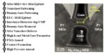
One of my favorite slides in the presentation is the Logic Scaling Roadmap slide and thankfully it is a figure in the paper (see figure 1.)

Figure 1. Logic Scaling Roadmap

For the 3nm node Imec shows a 5-track height cell based on a FinFET, this is the approach that I believe TSMC is taking. Samsung on the other hand has announced they will use Gate All Around at 3nm (a Horizontal Nano Sheet, HNS) and I believe this will be a 6-track height cell because to get to 5-tracks with HNS requires Buried Power Rails (BPR) and BPR is not ready for production yet (Samsung 3nm will be significantly less dense than TSMC 3nm based on the companies announced density improvements).

At 2nm, 5-track HNS utilizing BPR is an option or even HNS with a Fork Sheet (FS) to enable a less than 5-track cell (Authors note: ~4.33-tracks may be possible by combining HNS, BPR and FS).

Moving forward to 1.5nm CFETs with nFET and pFET stacking and 4-track cells can provide a shrink while maintaining the same pitches as 2nm. Imec is doing a lot of research on CFETs, Intel presented an interesting paper on CFETs at the conference that utilized three pFETs and two nFETs in a stack to match the performance of the two device types, and Synopsys also presented on CFETs in a paper that I was a coauthor on.

For 1nm and beyond Imec is working on 2D atomic channels and less than 4-track cells. There is also work that I am aware of to further extend CFETs by stacking more layers. 2D atomic channels would be stacked up like nanosheets but due to the extremely thin layers potentially provide higher frequency performance at the same power.

The presentation went on to further discuss BPR. BPR can lower the power delivery resistance improving power efficiency and provide an area reduction by creating tall metal lines in the substrate to replace wide metal lines in the interconnect layers. BPR can also enable power delivery networks on the back of a wafer that connect to BPR by using through silicon vias (TSV) although this requires very small “nano” TSVs. Utilizing the backside of the wafer for power delivery would also enable Metal Insulator Metal (MIM) Capacitors and Electrostatic Discharge (ESD) protection diodes to be integrated on the backside.

Beyond 2D atomic channel transistors, Imec is investigating various option including Qubits for quantum computing.

BEOL Roadmap

Looking at the Back End of Line (BEOL) Imec believes copper dual damascene can scale to a 21nm pitch but via resistance will be a problem. To address via resistance a hybrid scheme is needed where the vias are fabricated with an alternative material such as ruthenium, molybdenum, or tungsten. 3nm node processes are defined in the Imec roadmap as having pitches of 21-24nm so standard dual damascene copper is probably OK for the 3nm node. In the Imec roadmap the 2nm node has 18-21nm metal pitches so hybrid metallization will likely be required for the most critical layers.

Beyond 21nm pitch, subtractive metal patterning becomes attractive to enable high aspect ratio metal lines with partial or full air gaps to address line to line capacitance. Because copper is so hard to dry etch, subtractive metallization will require new metals such as Ruthenium or Molybdenum. The combination of Semi Damascene (with subtractive patterning) and air gaps results in a significant reduction in the resistance-capacitance (RC) of the interconnect. Imec has demonstrated 32nm pitch and is currently working on 18nm pitch. The initial 18nm results show better RC performance but still need work on self-aligned vias and air gap fabrication. Semi Damascene is a candidate for the 1.5nm node.

Beyond the 1.5nm node Imec is investigating alternative materials. The figure of merit for materials at very small dimensions is the bulk resistivity multiplied by the electron mean free path, this is because at small dimensions materials with long electron mean free paths, see a significant increase in resistivity. Imec has identified several promising alloys in simulations and needs to work through the integration challenges and demonstrate the materials are viable on actual devices.

SRAM Scaling

Continued logic scaling has been enabled by design technology co-optimization enabling track height reductions but this does not carry over to SRAM cells. Where SRAM cell sizes once scaled at 50% per node that scaling has slowed. A move to HNS will provide some gate length scaling but limitations on sheet width will limit scaling. FS can provide a scaling boost and CFETs can offer additional reductions.

There are also opportunities to utilize sequential 3D integration schemes and fabricate logic over SRAM arrays on pre-processed wafers, but this technique would require low temperature processing of the logic without compromising performance.

Deconstructed Chips

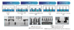
Increasingly capable 3D integration schemes offer the ability to deconstruct chips into multiple chips with each chip optimized for its function. Breaking up a complex system on chip (SOC) design into chiplets would allow optimized chiplets, for example one chiplet could be a processor core, other chiplets could be SRAM cache lower-level cache, MRAM or DRAM for higher levels cache or main memory all integrated with very high band width. Specialty devices fabricated with compound semiconductors could also be integrated. In order to realize the full potential of deconstructed 3D integration improvements in wafer to wafer bonding, micro bumps and power dissipation challenges need to be overcome.

Figure 2. illustrates Imec’s view of the 3D integration landscape.

Figure 2. 3D Integration Landscape.

 Conclusion

The technologies discussed here offer ten to fifteen more years of logic scaling. EUV patterning with the 0.33NA to High-NA (0.55NA) transition, HNS, FS, BPR, PDN, CFETs and 2D atomic channels, new SRAM scaling techniques and 3D Integration are all promising candidates for future logic technologies.

Also Read:

No Intel and Samsung are not passing TSMC

Leading Edge Foundry Wafer Prices

VLSI Symposium 2020 – Imec Monolithic CFET


The Growing Chasm in Electronic System Design

The Growing Chasm in Electronic System Design
by Rahul Razdan on 01-07-2021 at 10:00 am

supply chain block diagram

Since the formation of the Electronic Design Automation (EDA) industry in the 1970s, Moore’s law has increased functionality onto a semiconductor die dramatically.  In response,  EDA tools for semiconductor design have also grown in functionality and the design processes for semiconductors have moved forward at a breakneck pace. Interestingly, during the same timeframe, board design has largely stayed stagnant. Many of the major platforms for PCB design are decades old with specific additions in areas such as high-speed interconnect and advanced packaging.

Observation one: For the vast majority of system designers, PCB design today is not too dissimilar from the design process from the 1980s. 

Further, there is a large and growing chasm for system designers between consumer and non-consumer products. Consumer markets drive the level of volume which is very interesting for semiconductor companies. To support the consumer markets, semiconductor companies provide focused application resources and in some rare cases will even build custom silicon for the system provider.  However, the vast majority of system designers in very important markets (energy, defense, aerospace, and industrial) face an environment which is still dominated by the age old manual datasheet. The only real computer aid is the PDF textual search. Beyond the data sheet, the various important EDA artifacts of the chip such as mechanical structure, pinout, software drivers are disaggregated across vendors (often connected to EDA tool libraries) and must be chased down.  Overall, it is a very manual, tedious, and error prone process.

The major players in the semiconductor ecosystem (figure above) certainly have a desire to help their customers, and  there is an attempt to help system level designers with various capabilities.  These include:

  • Reference Designs:  Semiconductor vendors publish reference designs on their websites focused on communicating the proper way to use their chips.
  • Application Notes:  Semiconductor and other players often write application notes which discuss the applicability of electronics systems in particular vertical markets.

Observation 2:  There is a sea of information available on the internet, but it is distributed on a variety of websites in various non-standard ways. The only real automation mechanism available to a system designer is google search.  However, a generic textual search engine has its limitations in a semantically rich environment such as electronics system design.

Aggregators such as distributors certainly have made an effort to service system designers in the part selection process. Vendors such as Digikey and Mouser provide some insights on the availability of parts based on high level selection of hardware functionality on their websites.

Observation 3:  The part selection process is focused on semiconductor chips, so it does not provide clarity on the ability of other methods of implementing the same function. These might include sub functions in larger SoCs, programmable fabrics, software emulation, and more. This is simply not the focus of distributors today.

In fact, the fundamental design factors for most system designers such as operating environment, the vertical market certifications, important ecosystems (ARM, x86, etc), and useful lifetime of product are not addressed in any existing EDA system today. This leaves designers with the unenviable task of wading gingerly into an ocean of disorganized information. Further,  semiconductor chip design has a deep capability which defines and enforces design rules through the implementation of automated checks by EDA tools. This ranges from layout DRC to logical assertions.  PCB design systems certainly have some concept of layout DRC, but the higher levels of checks surrounding logical connections do not exist in the system board design suite.

Overall, the lack of automation at the system design level has an impact on designer productivity as well as correctness, and this is becoming an increasing problem. Why?

AI/IOT mega-trend:  As “The Coming Evolution in Electronics Design Automation” describes, the next big mega-trend is the move of electronics to the edge with sensor, analog, DSP, and cloud connected systems. A key enablement of this paradigm is a highly productive design capability.

The millennial designer: While datasheets may be the preferred method of communication for seasoned designers, the newer generation of designers expect a much higher degree of automation.

In conclusion, with the current productivity of the system design process, the limiting factor for semiconductor growth in non-consumer markets will increasingly become designer bandwidth. Much like semiconductor EDA, there is a need to invest in system design EDA capability to unleash the power of electronics to solve important societal problems in fields ranging from defense to sustainability. 

Also Read:

The Coming Evolution in Electronics Design Automation

The Increasing Gaps in PLM Systems with Handling Electronics

The Increasing Gap between Semiconductor Companies and their Customers


Conference: Embedded DevOps

Conference: Embedded DevOps
by Daniel Payne on 01-07-2021 at 6:00 am

embedded devops min

The catchy phrase DevOps is defined by Agile advocates as, “The practice of operations and development engineers participating together in the entire service lifecycle, from design through the development process to production support.

I’ve been developing software since the stone ages, which means that my first computer language in college was Fortran, and yes, we typed onto Hollerith cards and fed them into a Control Data card deck reader. A lot has changed since then, and I’ve since learned to code in many languages: BASIC, Fortran, Pascal, Assembly, C, ASP, Perl, Tcl/Tk, ColdFusion, PHP, HTML, Verilog, VHDL, Jquery, CSS, MySQL.

Perforce is well-known in the DevOps community, and they invited me to attend their upcoming webinar on February 4th, Embed DevOps, Summit 2021. So stay tuned for a detailed blog on one of the presentations. For now, let’s take a look at the three parallel tracks being offered:

  • Plan – Explore methodologies, tools, and practices that can help you cut costs in the planning stage of development.
  • Create – Learn how to improve things like collaboration, scaling, and versioning to reduce the time it takes to create a quality product.
  • Verify – Understand various practices that help you verify safety standards to reduce risk.

Plan

There are three sessions in this track that will help you explore methodologies, tools, and practices that can help you cut costs in the planning stage of development.

  • Scrum, Kanban, and Gantt Scheduling in One Project – Nonsense or Necessity?
  • Community vs. Enterprise Open Source – Which is Right for Your Business?
  • CWE Top 25: History, Tools and Techniques

Create

Four sessions are included in the Create track, which I plan on attending, and here you will learn how to improve things like collaboration, scaling, and versioning to reduce the time it takes to create a quality product.

  • Embedded Software Development at 5G Speed
  • Secure Collaboration in a Cloud-based Chip Design Environment
  • Optimizing Your CI Pipeline
  • Implementing a Unified HW/SW BoM to Reduce System Development

Verify

The third track has three presentations, and Verify will help you to understand various practices that help you verify safety standards to reduce risk.

  • CI Efficiency: How to Verify Every Developer Commit
  • Role of Coding Standards in Autonomous Vehicles
  • How to Improve Development with Strong Requirements Taxonomy

Presenters

Industry experts in each area will be at the virtual podium to bring us up to speed on embedded DevOps, and I’ve met two of them in real life: Vishal Moondhra of Methodics and Warren Savage, a researcher from the University of Maryland.

Summary

Mark your calendar for February 4th, then sign up early for the first virtual user conference from Perforce all about embedded DevOps. The conference is in good alignment with popular trends of: 5G, autonomous vehicles, cloud and open source software. As part of my continuous learning I’m looking forward to this conference next month, so why not join me.

Also Read:


Technology Optimization for Magnetoresistive RAM (STT-MRAM)

Technology Optimization for Magnetoresistive RAM (STT-MRAM)
by Tom Dillinger on 01-06-2021 at 6:00 am

profile simulations

Spin-transfer torque magnetoresistive RAM (STT-MRAM) has emerged from several foundries as a very attractive IP option.  An introduction to MRAM technology from GLOBALFOUNDRIES was provided in this earlier SemiWiki article. [1]

Briefly, STT-MRAM is a non-volatile storage option with the following attractive characteristics

  • high storage duration
  • high density (one access transistor connected to a magnetic tunnel junction)
  • random access
  • near-zero leakage power
  • radiation-hard
  • high-performance write cycle (with low write bit error rate)

There are limitations with STT-MRAM that require detailed process engineering:

  • thermal sensitivity of the energy barrier that defines the spin-polarization stability (“the exchange stiffness”)

A key application area for embedded MRAM qualification is the automotive market, with its more demanding -40C to 150C temperature environment.

  • limited endurance cycles

MRAM IP is targeted to displace embedded flash at more advanced process nodes – in this case, limited endurance is sufficient.  For applications such as the last-level cache in high-performance SoCs, higher endurance is required.

The nature of the STT-MTJ requires unique modeling and micro-magnetic simulation techniques to optimize the selection of materials and physical dimensions.  At the recent IEDM conference, GLOBALFOUNDRIES provided a perspective on the optimization of their MRAM technology offering. [2] This article summarizes their presentation.

Introduction

The magnetic tunnel junction (MTJ) consists of multiple ultrathin layers of unique metal and oxide materials, as illustrated in the figure below.


Recall that a material demonstrates magnetization due to the spin and orbit of its electrons.

A “soft” magnetic material only contributes to the magnetic flux around the material when an external magnetic field is applied – when the field is removed, there is no remnant magnetization.

A “hard” material is always magnetized.  When an applied magnetic field in the opposite direction of the magnetization exceeds a critical value, the polarity of the magnetization reverses, and remains magnetized in this orientation when the applied field is removed.  The magnetostatic energy in the hard material may differ based on the direction of the magnetization – i.e., a preferred direction in the absence of an external field – known as the magnetic anisotropy.

The configuration shown in the figure above is a perpendicular MTJ.  The materials selected for the junction provide for a perpendicular magnetic anisotropy (PMA), which enables a stable, non-volatile “anti-parallel” magnetic state between the reference and free layers.

The figure below depicts the perpendicular TMJ interface between the magnetic layer and the oxide – note in the figure that an “in-plane magnetic anisotropy” device is also depicted, but does not contribute to the PMA.

The perpendicular MTJ is emerging as the preferred material stack, for the following characteristics:

  • the PMA energy is larger for the p-MTJ than the in-plane anisotropy, with better retention at smaller MTJ sizes
  • the critical current density through the MTJ area to switch the magnetization is less for the perpendicular junction
  • as a result, the MRAM bitcell density may be much higher

The TMJ consists of a “reference” magnetic layer separated from a “free” magnetic layer by an extremely thin oxide.  The free layer magnetization is switched between anti-parallel and parallel orientations to the reference layer, with a corresponding change in the junction electrical resistance (measured at low “read” current).  The tunneling magnetoresistance ratio (TMR) achieved between the AP and P states is a key process development parameter, as it directly influences the memory read sense behavior.

The unique nature of the STT-MRAM cell is the manner in which the free layer magnetization is altered.

The angular momentum (“spin”) of an electron is normally random – thus, a conventional electrical current is non-polarized (1/2 spin-up, 1/2 spin-down).

However, an electron current through the reference layer produces a spin-polarized current through the tunnel oxide to the free layer.  The angular momentum of this electron current can be transferred to the free layer electrons, due to “spin-transfer torque”.  If the junction current magnitude is sufficient, the magnetic polarization of the free layer can be switched to parallel, as mentioned earlier for the case of an applied external magnetic field.

An electron current flowing in the opposite direction from the metal electrode re-orients the free layer magnetization to its anti-parallel orientation.

The first figure above also included “synthetic anti-ferromagnetic” (SAF) and metal spacer layers, as part of the MTJ stack.  These additional layers help to increase the TMR ratio and improve the stability of the cell.

STT-MRAM DTCO

The GLOBALFOUNDRIES team provided an insightful view into STT-MRAM development, as summarized in the pyramid diagram above.

The first step (lowest pyramid level) in MRAM development is the stack engineering of materials – e.g., crystalline structure, atomic composition, thickness, and interface properties at each layer boundary.  Detailed “spin-polarized” calculations are used to determine the follow material characteristics described earlier:

  • magnetic anisotropy (K)
  • magnetic saturation in the material (Ms)
  • TMR

For example, the figure below illustrates a calculation of the “energy barrier” associated with the free layer interface to the neighboring oxide – as mentioned earlier, the perpendicular anisotropy is of interest (so the in-plane magnetization polarization energy is subtracted).  The free layer in this example is a Cobalt-Iron (CoFe) material, roughly 10Angstroms thick; the tunnel oxide is MgO.

Recall from the discussion above that an increase in the PMA offers greater cell thermal stability and data retention – the adjoining figure above illustrates how this energy barrier changes based on the Co(x)Fe(1-x) material composition in the free layer.

An additional material analysis relates to modeling the spin-polarized electron tunneling current through the MgO oxide layer, as illustrated below.

The next level of the DTCO pyramid is to extend these electron-level, “ground-state, zero K” material simulations to include the temperature dependence of:  the material magnetic saturation (Ms); the magnetic anisotropy (K); and, the STT exchange behavior.

The figure below depicts how these properties change with temperature.  The data enable process engineers to determine how the PMA stability energy barrier varies with temperature, and ultimately to define the bitcell write cycle current and duration requirements for the temperature range of interest.

Note that the figure also includes an analysis of a “magnetic defect density” in the polarized material.  During fabrication and assembly, a SoC containing an embedded MRAM will be subject to elevated annealing temperatures – e.g., a minimum of 260C for solder reflow.  There will be some degree of non-magnetic layer atomic diffusion into the magnetic material.

The next level of the DTCO pyramid introduced the MTJ physical dimension into the process development.  The figure below illustrates how magnetic “coupling fields” are present in a tapered, non-fully cylindrical MTJ after fabrication.

The figure above also depicts how the magnetic coupling field in the free layer is a function of the MTJ diameter and thickness.  This external coupling introduces a dimensional asymmetry in the overall free layer-oxide interface, complicating the modeling of the parallel/anti-parallel switching behavior.  A high field coupling at the periphery slows the write transition for either the P-to-AP or AP-to-P magnetization orientation.  A detailed analysis is required to optimize the MTJ dimensions – large enough to avoid coupling-impacted write transition errors, yet still achieving array density and switching power targets.

The final, top level of the DTCO pyramid is the abstraction of the previous analyses of materials, temperature-dependence, and MTJ dimensional analysis into a suitable “compact device model” useful for MRAM array designers to incorporate with the SPICE models for array decode, bitcell access transistor, write driver, and read sense devices.

The success of the final compact model generation is depicted in the figures below.  The first illustrates the (AP and P) DC resistance measured versus model for two different MTJ stack designs.  The second figure depicts the interdependence between the required write pulse magnitude and duration, again showing excellent agreement between the compact model and measured MRAM hardware.

As highlighted above, the profile of the overall MTJ alters the coupling field to the switching free layer.  The DTCO flow developed by GLOBALFOUNDRIES includes a statistical compact model, reflecting the process variation in the MTJ, and thus the coupling field.

The figure below illustrates the results of a Monte Carlo simulation analysis of the MRAM, using the compact model incorporating a statistical distribution of the coupling field.  Again, excellent agreement with measured hardware is shown, when simulating the overall write error rate (“WER”), for a 20nsec write pulse width.  (Note that when a short write pulse ends, there is a probabilistic measure that the free layer may “relax” back to its existing state, constituting a write error.)

As an experiment, an artificial statistical distribution (“B”) for the MTJ profile and resulting coupling field was simulated, showing the strong dependence between MTJ process variation and WER.  MRAM fabrication engineers are focused on improving the MTJ layer etch definition, to achieve better WER and correspondingly improved overall write cycle endurance.

Summary

GLOBALFOUNDRIES presented an extremely enlightening view into the complete DTCO flow for STT-MRAM development.  Material characteristics are analyzed across (ground state and high-temp) conditions, resulting in input parameters used at higher levels of model abstraction.  The influence of manufacturing variation – e.g., MTJ sidewall taper, material defect densities – were also incorporated into the overall model environment, due to the influence of coupling fields on MTJ behavior.  The resulting compact models used in a traditional circuit design flow demonstrated excellent agreement with experimental hardware data.

I would encourage you to seek out a copy of the IEDM presentation from GLOBALFOUNDRIES to gain insights into the DTCO steps involved in MRAM process engineering.

-chipguy

References

[1]  https://semiwiki.com/semiconductor-manufacturers/287266-embedded-mram-for-high-performance-applications/

[2] Dixit, H., et al, “TCAD Device Technology Co-Optimization Workflow for Manufacturable MRAM Technology”, IEDM 2020, paper 13.5.

Also Read:

3DIC Design, Implementation, and (especially) Test

Designing Smarter, not Smaller AI Chips with GLOBALFOUNDRIES

The Most Interesting CEO in Semiconductors!


The Coming Evolution in Electronics Design Automation

The Coming Evolution in Electronics Design Automation
by Rahul Razdan on 01-05-2021 at 10:00 am

Electronics MegaTrends

Electronics design mega-trends have been a transformational force for the world. As shown in blue in Figure 1, the first wave of electronics consisted of centralized computing and the leaders in the field included companies such as IBM, Digital Equipment Corporation (DEC), Wang, and others.  Fundamentally, these technologies provided productivity solutions for the administrative (G&A) functions for the global business enterprise. With this shift, the finance, human resources, and administrative functions of global business were disruptively impacted.  Gone were the days of a sea of admins doing paperwork.

Figure 1: Mega-Trends (Anew-da.ai)

Electronic Design Automation was born inside the large companies such as DEC as well as flagship university institutions such as UC Berkeley before spinning out into an independent industry. Initially, EDA for system design (PCB) and semiconductor design were of similar size. However, as Moore’s law drove increasing functionality onto a semiconductor chip,  EDA tools for semiconductor design scaled accordingly.  Over the last 50 years, semiconductor design has grown to dominate the business of EDA. 

The next wave consisted of edge computing devices (red in Figure 1) such as personal computers, cell phones, and tablets. With this capability, companies such as Apple, Amazon, Facebook, Google, and others could add enormous productivity to the advertising and distribution functions for global business. Suddenly, one could directly reach any customer anywhere in the world. This mega-trend has fundamentally disrupted markets such as education (online), retail (ecommerce), entertainment (streaming), commercial real estate (virtualization), health (telemedicine), and more. In terms of design, the big shift was the focus on mobile battery based devices in highly integrated cost-sensitive products.  To support this new system paradigm, the EDA design chain had to be updated to understand and support a wide variety of methods which minimized power dissipation. In addition, supporting integrated mechanical, packaging, system design became a necessity. 

What is the next mega-trend and what does it imply for the required evolution of EDA capability ?

Today, we are at the beginning of the next major disruptive cycle caused by electronics. This cycle consists of embedded sensory devices (sometimes known as Internet of Things), local intelligence systems (sometimes known as machine learning), and global intelligence (sometimes known as cloud resources). Broadly called AI/IoT, these three technologies will disruptively impact nearly every market segment where in-field sensing with computing can solve interesting problems. Medical devices, mining, agriculture (land or ocean), space operations, and of course autonomous vehicles, are rich examples of this paradigm.

Table 1: Short LifeCycle (SLC) vs Long LifeCycle (LLC) (Anew-da.ai)

AI/IOT moves electronics onto the “edge” and also into the world of Long LifeCycle (LLC) products. Table 1 contrasts the system level characteristics between short and long cycle products.  Similar to the shifts in previous mega-trends, the AI/IOT paradigm requires EDA to support several new capabilities. These include:

  1. Design for Supply Chain Resilience:  Today, the semiconductor supply chain is dominated by SLC products, and this is not expected to change. LLC products face a circumstance where they need to design in such a manner as to absorb the enormous churn created by the SLC products on the semiconductor supply chain.
  2. Design for Reliability:  Today, most of the semiconductor supply chain is optimized for the consumer life cycles. To gain the required reliability characteristics for long cycle products one must build the reliability through system design techniques.
  3. Design for Functional Evolution:  Many LLC products are embedded in the field with high replacement costs (ex.. smart buildings). The probability for requirements evolution over time is very high, so designing for functional evolution is another key requirement of this product segment.
  4. Design for System Maintainability:  Field maintainability is a key issue for LLC products. Thus, key ideas such as automatic calibration of sensors or automated detection of fault becomes very important in this design space. 

Many of these issues have existed for many years in markets such as satellites and indeed agencies such as NASA have invested in internal solutions. However, similar to spinout from large information technology OEMs from the 1980s, there is a need for commercial EDA solutions to support the LLC design paradigms.

For those interested in further reading on these topics:

  1. Let’s Define Long Lifecycle (LLC) Electronics Markets
  2. LLC Markets and the Electronics Supply Chain
  3. LLC Markets and the AI/IOT Mega Trend
  4. Obsolescence Insurance, a New High-Margin Business for EMS Companies
  5. LLC Markets, the PCB ASIC Model and EMS
  6. Reconfigurable Computing and LLC Markets

Also Read:

The Growing Chasm in Electronic System Design

The Increasing Gaps in PLM Systems with Handling Electronics

The Increasing Gap between Semiconductor Companies and their Customers


PLDA is at the Leading Edge with Advances in Both PCIe 5.0 and CXL

PLDA is at the Leading Edge with Advances in Both PCIe 5.0 and CXL
by Mike Gianfagna on 01-05-2021 at 6:00 am

PLDA is at the Leading Edge with Advances in Both PCIe 5.0 and CXL

There are significant advances in communication protocols happening all around us. The Peripheral Component Interconnect Express (PCIe) Gen 5 standard is delivering the needed device-to-device performance to support artificial intelligence and machine learning applications as well as cloud-based workloads. The rapidly evolving Compute Express Link (CXL) standard is delivering CPU-to-device and CPU-to-memory communication to enable next-generation data center performance. Both are critical enablers for next generation systems and require support in the form of semiconductor IP to be deployed. PLDA has made recent announcements regarding significant milestones for both PCIe and CXL, which is not a common occurrence. I wanted to look a bit closer at both of these announcements to see how PLDA is at the leading edge with advances in both PCIe 5.0 and CXL.

Both announcements were covered on SemiWiki. One is about the demonstration of successful PCIe 5.0 link training with PLDA’s PCIe 5.0 controller and Broadcom’s PHY. The other is about successful CXL interoperability with the pre-production Intel Xeon CPU, code named Sapphire Rapids. Standards support is all about interoperability and both of these announcements deliver proof of PLDA IP interoperability. Let’s take a closer look.

PCIe 5.0

What was announced here was a demonstration showcasing a stable PCIe 5.0 link training (32 GT/s) featuring excellent signal integrity with a Broadcom® PCIe 5.0 PHY. PLDA used its XpressRICH® IP Controller for PCIe 5.0 with Broadcom’s PCIe 5.0 PHY IP. Several different scenarios were presented to highlight the exceptional signal integrity of the combined IPs. PLDA explained that the demo serves as a quality guarantee for SoC designers using the combined solution of PLDA’s PCIe 5.0 controller and Broadcom’s PHY IP.

The demonstration included:

  • Exceptional signal integrity via an eye scope provided by a SerDes pattern generator and PCIe 5.0 Tx compliance patterns monitored on a scope
  • Stable PCIe link training at 32 GT/s proven by a crosslink connection of two boards monitored using Xilinx Vivado ILA and a Viavi PCIe analyzer
  • Backward PCIe compatibility at 16 GT/s, 8 GT/s, 5 GT/s, 2,5 GT/s that were demonstrated in a real environment

Stephane Hauradou, CTO at PLDA commented, “It’s a great milestone for PLDA technical teams to achieve stable PCIe Link Training at 32 GT/s. The complexity and the challenges involved in reaching this result have evolved with the different PCIe generations and we wanted to further demonstrate our PCIe 5.0 solutions, even though they are already proven in silicon.”

There is also a video available here that allows you to see the demo in action.

CXL

The CXL announcement was also about performance and interoperability.  This time, between PLDA’s XpressLINK™ CXL IP, running on a PLDA FPGA-based add-in card and Intel’s development platform equipped with pre-production “Sapphire Rapids” processors. The PLDA XpressLINK controller implements the CXL.io, CXL.cache, and CXL.mem sub-protocols as specified in the recently released CXL 2.0 specification and is already being designed-in at leading technology companies.

The demonstration was conducted at Intel’s Industry Enabling Labs as part of a long-term collaboration between PLDA and Intel’s industry enabling group. Stephane Hauradou commented, “Today’s demonstration of interoperability between PLDA’s XpressLINK CXL IP, which delivers the lowest latency in the industry, and a cutting-edge CPU like pre-production Intel Sapphire Rapids processor, is a critical step in assuring SoC designers of the robustness of our CXL implementation”.

Dr. Debendra Das Sharma, Intel Fellow and Director of I/O Technology and Standards Group, Data Center Group also commented, “CXL will be a foundational interconnect technology in the data centers and networks of the future. The availability of third party silicon IP like the PLDA XpressLINK CXL Controller IP lowers integration risks and helps ensure quicker proliferation of the CXL protocol across the industry ecosystem.”

PLDA XpressLINK and XpressLINK-SOC CXL IP are highly parameterized CXL controller soft IP designed to the latest CXL specification and architected for SoC, ASIC, and FPGA implementation. XpressLINK and XpressLINK-SOC are available for licensing immediately and are already designed at several leading-edge technology companies.

Summary

PLDA is a technical leader in high-speed Interconnect IP. These two recent announcements separated by only a few weeks demonstrate their commitment to supporting the latest standards with a focus on interoperability and robustness. To probe further:

PCIe

CXL

You will clearly see that PLDA is at the leading edge with advances in both PCIe 5.0 and CXL.


Author Interview: Bernard Murphy on his latest book

Author Interview: Bernard Murphy on his latest book
by Daniel Nenni on 01-04-2021 at 10:00 am

The Tell Tale Entreprenuer

Over the last 40 years, Bernard has worked with semiconductor and EDA companies in hands-on, management and consulting roles in engineering, sales and marketing. He most recently co-founded Atrenta where he created and led the development of SpyGlass, retiring as CTO when Atrenta was acquired by Synopsys. Post-retirement, he’s been an active blogger for SemiWiki. He’s also written a couple of books under the SemiWiki label and he independently advises a number of clients on marketing content

Why did you decide to write The Tell-Tale Entrepreneur?

Over the last 40 years, I’ve created, suffered and edited more than my fair share of biz and tech communication. Which has reinforced my view, widely shared, that our communication is pretty bad. Pitches, blogs, white papers aiming to convince are at best unconvincing, at worst painful. What’s curious is that, from engineers to CEOs, think we’re good at PowerPoint. Yet we’re terrified at the thought of writing. PowerPoint feels like a familiar template, communicate-by-numbers. Word has no template; we have to start from a blank sheet, hence the terror. Which suggests the format is beside the point, we suck at communication either way. PowerPoint just lulls us thinking we don’t.

I started out just as bad, but I worked hard to improve. Through a lot of trial and error I believe I figured out the problem. I want to pass this on, not through a boring how-to book but through an entertaining set of short stories. Designed to show you how to make your communication just as engaging.

How is storytelling different and why is it better than other ways to communicate?

Take PowerPoint as a reference. It’s well established and has great value in structured contexts where efficient information transfer is the goal. Status updates, project planning, training, technical due diligence. But it’s weak in persuasion. Where you need to convince a client, prospect, investor that you have the best product for their needs. Or you are their best possible partner. Or you failed to deliver what you promised and now must rescue the relationship.

These are times when slides are the wrong answer. You have to connect emotionally with your audience – building excitement around a new direction, dealing with fear of possible failure, maybe pointing out pitfalls that you already understand well. Or convincing them there will be no more mistakes. Eyeball to eyeball conversations.

The best way to guide that conversation is through a story. You’re looking at them (not slides), they’re looking at you, and you’re telling them a story, appealing to their emotions.

Storytelling isn’t a new idea. What makes your approach different?

Storytelling is a very old idea. Today we relegate stories to entertainment, expecting that business communication needs a more professional approach. Our brains don’t agree. We’ve been telling stories from beginning of time. Not just to entertain but also to pass on wisdom, culture, beliefs, laws. Our brains are wired to receive stories efficiently, motivating us to action. Not so for data and logic dumps. That’s why we find PowerPoints so boring and start scrolling through texts, emails, anything rather than listen to the speaker.

Instead tell a story. Stories are naturally engaging, especially when they sound roughly relevant to the audience’s goals. We want to know what’s going to happen next. Calling the hero to adventure. Facing tests together, proving ourselves a worthy mentor. The big challenge where it could all go wrong, but somehow our hero makes it through, now stronger, more capable. And the final challenge. Much more interesting than texts and emails. They learn what you can do for them along the way, in a context they recognize.

Storytelling is big in marketing now. Tons of advice online on how to do it – blogs, whitepapers, companies who want to advise you (for a fee). But there’s something a bit odd about this advice. It all seems to come in the same business communication standard format: explanations, bullet lists and charts. You want to learn how to tell stories. Wouldn’t it be better to do that by reading stories?

That’s my innovation – I explain how to tell stories by telling you stories.

Who do you think will find value in this book?

Anyone in tech who must communicate with customers, prospects, investors. Who wants to reach markets through blogs and white papers. Those who aspire to sell their company. All will relate to experiences in these stories. And will I hope will be inspired to re-imagine and improve their own stories, based on these examples.

The book is also written for a general audience. Anyone interested in real stories drawn from different phases in the lives of tech ventures. Technology plays a role in these stories but isn’t primary, so I’ve simplified quite a lot. People, opportunities, challenges, growth are the most important elements.

These stories are for everyone, but especially for us communicators in tech. Most important, I hope you will begin to understand why our audiences are thirsting for stories, not more death-by-PowerPoint.

Where can we find the book?

The Tell-Tale Entrepreneur is available for pre-order on Amazon and will be released on January 26th, 2021.


Optimization for pFET Nanosheet Devices

Optimization for pFET Nanosheet Devices
by Tom Dillinger on 01-04-2021 at 6:00 am

Intel flow TEM

The next transition from current FinFET devices at advanced process nodes is the “nanosheet” device, as depicted in the figure below. [1]

The FinFET provides improved gate-to-channel electrostatic control compared to a planar device, where the gate traverses three sides of the fin.  The “gate-all-around” characteristics of the nanosheet device provide further improvements in electrostatic control, surrounding the device channel.  This is typically reflected in a more optimal subthreshold slope, or SS.  The SS relates to the change in device gate input voltage that results in a factor of 10X change in leakage current.  A smaller SS implies both faster device switching and, significantly, a reduction in the static source/drain leakage current and leakage power dissipation.  (More on SS shortly.)

Additionally, the nanosheet device offers more design flexibility.  Whereas the topology of the FinFET device width is quantized (Weff ~ ((2*fin_height) + (fin_thickness))), the width of the nanosheet device is defined by EUV lithography (Weff ~ nanosheet_perimeter).

The effective nanosheet width can be further extended by stacking multiple channels vertically, with the gate material fully surrounding each of the individual nanosheets.  The design flexibility and improved device characteristics make this technology option very attractive.

There are major challenges to the introduction of nanosheet processing to production, however.  Here are but a few:

  • isolation of individual “ribbons” of the nanosheet device channel

The nanosheet device is fabricated in an epitaxial layer.  The horizontal device sheet is embedded within other epitaxial-grown layers – e.g., a silicon layer sandwiched by epitaxial layers of different composition, such as SiGe/Si/SiGe/Si/SiGe.  (As will be described shortly, the close similarity in crystalline structure between Si and Ge is critically important.)

The formation of the nanosheet device “ribbon” requires a very selective etching process.  The epitaxial layers above and below are to be removed, while not etching the remaining device channel.  For multiple, stacked nanosheets, this etching process also needs to be anisotropic, so that all the sacrificial epitaxial layer material between nanosheets is fully removed.

  • the high-K gate oxide dielectric surrounding the exposed nanosheet ribbons needs to be extremely uniform, with excellent adherence

The oxide defect density and interface trap density (for injected “hot” carriers) needs to be extremely low.  (An annealing step in a hydrogen gas environment is commonly included as part of the device process flow.)

  • similarly, the metal gate material stack needs to be deposited uniformly throughout the structure, fully enclosing the stacked sheets

The gate stack is typically comprised of an initial metal-to-oxide “workfunction” layer (e.g., TiN), followed by a metal to fill the gate volume, such as Tungsten.  (Atomic layer deposition (ALD) is truly an amazing technology.)

  • a low resistance source/drain device node needs to be fabricated adjacent to the channel, to reduce Rs and Rd

An epitaxial growth step (with a high dopant concentration) is used to increase the S/D volume next to the channel, suitably isolated from the gate by a sidewall separation oxide.  (Other FET topologies also use a similar raised S/D epitaxial step.)  Additionally, the S/D doping profile needs to ensure a low contact resistance to the first-level metal.

  • “device engineering” needs to introduce significant strain into the channel material, to improve the free carrier mobility, and thus, the drive current

For several process generations, from planar to FinFET device topologies, various techniques have been employed to introduce strain into the channel material crystal – tensile strain for higher nMOS electron mobility, compressive strain for higher pMOS hole mobility.  “Stressor” material dielectric layers were added on top of planar devices.  The raised S/D epitaxial regions also transfer strain to the channel.

Of particular concern is the disparity between the electron and hole mobility in silicon.  Process development engineers continually strive to improve the hole mobility, to bring it closer to the electron mobility.  A key advance in this area has been the addition of Ge to the S/D epitaxial growth step, and ultimately, to the pFET channel – i.e., a Si(x)Ge(1-x) crystalline structure, providing a compressive strain and vastly improved hole mobility.  (Seasoned circuit design veterans will remember the days when pFET device widths were 2.5X-3X the nFET device width, to compensate for the hole versus electron mobility disparity.  With strain introduced during SiGe pFET fabrication, that difference is vastly reduced.)

The transition to a nanosheet channel of very small thickness exacerbates the difficulty in providing improved pFET device characteristics.  At the recent IEDM conference, Intel presented a detailed paper on how their nanosheet engineering has addressed this challenge. [2]  The rest of this article summarizes the highlights of their presentation.

pFET Nanosheet Fabrication

An overview of the nFET and pFET nanosheets are depicted in the figure below.

(The focus of the IEDM Intel presentation was on pFET engineering.)

As mentioned above, compressive strain in the channel is key to a high-performance device.  This is achieved by the following:

  • the epitaxial nanosheet for the pFET channel is Si(0.4)Ge(0.6)
  • the raised S/D epitaxial growth volume is also SiGe
  • the substrate directly below the nanosheet consists of Si and a “strain relief buffer” (SRB) layer of Si(0.7)Ge(0.3)

This buffer layer offers an intermediate crystalline transition from the bulk silicon substrate, and provides some degree of additional channel strain.

Parenthetically, the crystal lattice constants of Si and Ge differ by only 4.2% — Si = 0.543nm, Ge = 0.566nm.  As a result, the Ge/Si ratios are fully miscible.

The figure above also illustrates other process engineering constraints:

  • a highly doped top layer on the S/D regions is required for low contact resistance
  • the gate oxide needs a low defect and trap density (with a very aggressive high-K material thickness – e.g., an interface dielectric to the channel and a subsequent HfO2 layer)

The transition from the nanosheet thickness (~5nm) to large p+ S/D nodes requires detailed process engineering, to electrically isolate the gate from the S/D, and introduce compressive strain into the pMOS channel from the doped SiGe epitaxy.  (More on this step shortly.)

The figure below summarizes the overall Intel pMOS nanosheet fabrication steps, and provides a TEM cross-section of a single nanosheet device – NS thickness = 5nm, Lgate = 25nm, width = 100nm, EOT oxide = 9.1Angstroms.

Nanosheet fabrication requires several unique steps, combining conformal materials deposition with both isotropic and anisotropic (directional) etch technology.  Additionally, the isotropic etch technology needs to be very selective to different materials composition.

The figures below from Reference [3] illustrate an overall flow for the general case of multiple stacked nanosheets.  (The Intel IEDM discussion focused on materials and compressive channel strain for a single pMOS nanosheet device.)

The starting material is alternating layers of undoped Si/SiGe epitaxy.  A “dummy” top-level gate is patterned, followed by conformal deposition of an oxide and (highly) anisotropic etching of the oxide and Si/SiGe layers to form the starting nanosheet stack.  The next steps are critical, as depicted below.

The sidewalls of the exposed gate areas are selectively etched, to provide a recessed volume for conformal oxide deposition.  Anisotropic etching of this oxide results in a stack where the gate areas have lateral spacer oxide, while the sidewalls of the channels remain exposed, and serve as the seed for source/drain epitaxial growth.

Nanosheet nMOS devices in Si require processing with highly selective etching of the adjacent SiGe layer, exposing the Si sidewall for S/D epi growth.  Nanosheet pMOS devices require high etch rates of Si, exposing the SiGe sidewall for S/D epi growth.  Extensive process R&D (and materials chemistry) has been applied to optimize the Si/SiGe “etch rate ratios”.

After S/D epi growth, the dummy gate and epitaxial gate layer are etched away (again, very selectively to the now released nanosheet channel “ribbons”).  After a pre-clean, the high-K gate oxide materials are deposited on the ribbons, followed by the (workfunction and low-resistance) metal gate stack, both steps using atomic-layer deposition (ALD).  Contact “trenches” down to the bottom nanosheets are opened and filled with metal, completing the nanosheet fabrication.  (There are chemical-mechanical polishing (CMP) steps in this flow, as well, for surface planarity prior to etching.)

Parenthetically, it should also be mentioned that extensive process R&D has been invested to select the specific crystalline orientation that optimizes the strain-enhanced carrier mobility, etch rate selectivity, and S/D epitaxial growth.

Nanosheets and the parasitic transistors

Returning to the Intel presentation for their optimized compressive strain pMOS nanosheet, IDS-VGS curves for different devices are shown below (Lgate = 55nm and 25nm).

As might be expected from the superior electrostatics of the gate-all-around configuration, the subthreshold slope measured for these devices is exceptional.  (Intel did not describe their engineering approach toward establishing the threshold voltage of the pFET device.)

Of particular interest is the behavior at the S/D-to-substrate interface.  The nanosheet structure results in a parasitic transistor between the metal gate surrounding the bottom nanosheet and the substrate.  The S/D contact to the nanosheet also serves as the S/D connection for the bottom parasitic transistor.  To evaluate the magnitude of this parasitic device current, Intel fabricated and measured a test vehicle consisting of only this parasitic transistor – the experimental results are shown below.

The leakage currents from this device are much less than for the nanosheet, indicating suitable suppression of this “sneak” current.  (To further reduce this parasitic current, a punchthrough stop dopant region could be introduced below the S/D contact.)

VDD Optimization

For high-performance applications, designers are seeking to boost the supply voltage toward the technology maximum.  The limitations are due to the increased Ioff leakage at higher voltages.  A higher drain-to-source electric field in the channel result in drain-induced barrier lowering (DIBL) current, and very high drain-to-gate fields result in gate-induced-drain-leakage tunnel current (GIDL).   The figure below indicates that VDD = 0.9V is feasible for this technology, before the GIDL current increases exponentially (strained-SiGe, Lgate = 25nm, t_NS = 5nm).

Summary

Nanosheet devices are the next evolution in advanced process nodes after FinFETs.  Yet, nanosheet fabrication requires several unique process steps – e.g., ALD, epitaxial growth, and highly selective etch rate ratios.  Of specific concern is the requirement to introduce compressive strain in the pMOS nanosheet channel, to improve the hole mobility.  A unique combination of Si and Si(x)SiGe(1-x) material layers and epitaxy are required.  Intel recently discussed their results on optimizing pMOS nanosheet engineering.  I would encourage you to review their presentation.

-chipguy


References

[1]  Jeong, J., et al, “Comprehensive Analysis of Source and Drain Recess Depth Variations on Silicon Nanosheet FETs for Sub-5nm Node SoC Application”, IEEE Access, Volume 8, 2020.

[2]  Agrawal, A., et al, “Gate-All-Around Strained Si0.4Ge0.6 Nanosheet PMOS on Strain Relaxed Buffer for High Performance Low Power Logic Application”, IEDM 2020, paper 2.2.

[3]  Cheng, K., et al., “Nanosheet with Changing SiGe Percentage for SiGe Lateral Recess”, US Patent No. 10,312,350B1, June 4, 2019.


Podcast EP1: Why are Semiconductors so Sexy?

Podcast EP1: Why are Semiconductors so Sexy?
by Daniel Nenni on 01-01-2021 at 10:00 am

The goal of this Podcast Series is to bring semiconductor experts together to get to the truth about the matter at hand. We’ll get right to the point and not exceed 30 minutes of your time. If you have a topic you would like us to cover please post it on SemiWiki.com and we will get right to it.

After introductions from Daniel Nenni and his podcast partner Mike Gianfagna, Dan and Mike discuss the high profile semiconductors enjoy today. This bright spotlight is a relatively recent phenomenon.  How the semiconductor market began and what forces shaped the current climate are discussed. Many of these topics will be the subject of future episodes.

The views, thoughts, and opinions expressed in these podcasts belong solely to the speaker, and not to the speaker’s employer, organization, committee or any other group or individual.