RVN! 26 Banner revised (800 x 100 px) (600 x 100 px)

Podcast EP33: Processing AI Workloads

Podcast EP33: Processing AI Workloads
by Daniel Nenni on 08-13-2021 at 10:00 am

Dan and Mike are joined by Dana McCarty, vice president of sales and marketing at Flex Logix Technologies, Inc. Using an eFPGA-based architecture for processing AI workloads is discussed, along with typical applications and power, performance and cost benefits. The competitive positioning of Flex Logix’s InferX X1 are reviewed, along with the methodology to implement AI workloads with the part.

Dana is responsible for InferX X1 software, silicon and systems products. He holds a BSEE, University of Texas at San Antonio. Dana started writing software as a test engineer at AMD. He transitioned into sales holding senior management and then executive roles in both the USA and globally for Broadcom, Maxlinear, Teradyne and ARM. Dana has lived for eight years in Taiwan and China.

Flex-Logix are gold partners at this year’s 4th Annual AI Hardware Summit, held in California and online from September 13-16. The Summit’s mission is to help those accelerating AI workloads in the cloud, and at the edge, with this year all about systems level AI acceleration. Quote SEMIWIKI10 to save 10% on all passes.

View the agenda brochure here:  https://hubs.ly/H0Vkbf90

The views, thoughts, and opinions expressed in these podcasts belong solely to the speaker, and not to the speaker’s employer, organization, committee or any other group or individual.


TSMC Explains the Fourth Era of Semiconductor – It’s All About Collaboration

TSMC Explains the Fourth Era of Semiconductor – It’s All About Collaboration
by Mike Gianfagna on 08-13-2021 at 6:00 am

TSMC Explains the Fourth Era of Semiconductor – Its All About Collaboration

The 32nd VLSI Design/CAD Symposium  just occurred in a virtual setting. The theme of the event this year was “ICs Powering Smart Life Innovation”. There were many excellent presentations across analog & RF, EDA & testing, digital & system, and emerging technology. There were also some excellent keynotes, and this is where I’d like to focus. TSMC’s Suk Lee presented a keynote entitled, “Moore’s Law and the Fourth Era of Semi”.  Anything that attempts to make sense out of the storied and turbulent history of the semiconductor industry catches my attention. As explained by TSMC, the fourth era of semiconductor is all about collaboration. Let’s a take a closer look.

The keynote was presented by Suk Lee, vice president, Design Technology Platform at TSMC. I’ve known Suk for a long time, so this presentation was a must-see for me.  I sold to Suk when I was at Zycad and he was at LSI Logic. That was challenging as Suk is not easily impressed. I then worked with Suk at Cadence where we achieved some great results. His high bar for technical excellence was alive and well and it helped us. Since Cadence, I’ve had a few gigs in companies that were part of the Design Technology Platform Suk oversees at TSMC. Again, meeting his high bar for technical excellence made us all better. Let’s look at the history of the semiconductor industry, according to TSMC and Suk Lee.

The First Era of Semiconductor – IDM

To begin with, the transistor was invented at Bells Labs, followed by the first integrated circuit at Texas Instruments. Things got really interesting when the first monolithic integrated circuit was developed at Fairchild. The photo below, courtesy of the Computer History Museum shows some of the early pioneers involved in this work. You will recognize their names. Note everyone is wearing a jacket and tie. This might be something to think about as you plan your return to the office.

Fairchild pioneers

And so, the first era of semiconductor was born – the Era of the integrated device manufacturer, or IDM. These were monolithic companies that did it all – chip design, design infrastructure, chip implementation and process technology. I started my career in the design infrastructure area at an IDM called RCA. Suk points out that integration and invention went hand-in-hand at IDMs. The opportunity to create something completely new was quite exciting. I know that from first-hand experience. Custom chips were the domain of IDMs. They had all the infrastructure, technology and staff to get it done. And so custom chips were limited to IDMs or companies with enough money to fund the massive development at an IDM. That all changed when we got to the second era of semiconductor.

The Second Era of Semiconductor – ASIC

Companies like LSI Logic and VLSI Technology were the pioneers for this phase. Now, design infrastructure, chip implementation and process technology were provided to all by the ASIC vendor. The semiconductor industry began to disaggregate during this time. Armed with design constraints, a much broader community of engineers could design and build a custom chip. The technology became democratized, and the world was never the same.

The Third Era of Semiconductor – Foundry

The third era is essentially a maturation of the second era. All of the steps in IC design and fabrication are quite challenging. Assembling an ecosystem where each company focuses on their core competence is a great way to manage complexity. This is what happened in the third era. Chip design and implementation were addressed by fabless semiconductor companies, design infrastructure was delivered by EDA companies and process technology was developed and delivered by foundries. TSMC was a key pioneer for this phase.

The Fourth Era of Semiconductor – Open Innovation Platform

Watch carefully, we’re about to come full circle. As the semiconductor industry continued to mature, process complexity and design complexity began to explode. Esoteric and subtle interactions between process technology, EDA, IP and design methodology became quite challenging to coordinate with a disaggregated supply chain. TSMC was the pioneer for this era as well.

The company realized that a substantial amount of coordination and communication was needed between the various parts of the disaggregated ecosystem. A way to bring the various pieces closer together to foster better collaboration was needed. And so, TSMC developed the Open Innovation Platform®, or OIP. They began this work early, when 65 nm was cutting edge. Today, OIP is a robust and vibrant ecosystem.

The infrastructure provided by TSMC paved the way for improved collaboration and coordination, creating a virtual IDM among its members. This provides TSMC’s customers the best of both the monolithic and disaggregated models. It changed the trajectory of the semiconductor industry and provided TSMC with a substantial competitive edge.

There are many benefits of the model. The ability to perform design technology co-optimization (DTCO) is one that is quite useful. The figure below illustrates the breadth of TSMC’s OIP. Advanced semiconductor technology requires a village, a big village.  To help decode some of the acronyms DCA stands for design center alliance and VCA stands for value chain aggregator.

TSMC OIP®

We’ve now reached the end of the semiconductor history lesson, for now. Getting to this point has been quite challenging and exciting. Suk Lee did a great job explaining the history. TSMC made it happen and we’re better as a result. I look forward the next phase of semiconductor growth and where it may take us. For now, remember that the fourth era of semiconductor is all about collaboration.


Synopsys’ Complete 800G Ethernet Solutions

Synopsys’ Complete 800G Ethernet Solutions
by Kalar Rajendiran on 08-12-2021 at 10:00 am

Evolution of Ethernet Speeds

If I ask the question, “What has grown 4,000x over the last twenty-five years?”, most people will start throwing names of some stocks. Although various stock markets have had crazy run ups and yes, there is a stock that has grown 2,500x over that period of time, the answer to the 4,000x question is not a stock. What if I modify the question and ask “what has grown an average 2x every 2 years over the last twenty-five years?”, Moore’s law may pop up in many people’s mind. But the answer to both the questions is Ethernet speed evolution. We all benefit from it on a daily basis and have come to take high-speed networking for granted.

Figure: Evolution of Ethernet Speeds

Source: Synopsys

Even without any competing communications standards, Ethernet speed evolution has kept a nice pace, driven by the IEEE 802.3 standards committee and working group. This vigor got a boost in 2014 when Arista, Broadcom, Google, Mellanox and Microsoft formed the 25G Ethernet Consortium. The motive was to get to 25G quicker than what the Ethernet standards committee’s roadmap was showing at that time. Progress has been so rapid that the name has already gotten outdated. The consortium recently rebranded itself as the Ethernet Technology Consortium, so that it does not have to look for another name every time the next goal is achieved. The consortium now boasts of 45+ members representing various aspects of the ecosystem. And the consortium rolled out the 800GbE specification in 2020.

The need for speed is driven by Hyperscale Data Centers that are needed to support the rising data rates required to process high-performance workloads such as cloud computing, deep learning, 5G and video streaming applications. And the data centers are built with scalable network architectures such as the 2-tier leaf-spine architecture shown in the figure below.

Figure: Leaf-and-spine Architecture

Source: Synopsys

The leaf-spine architecture requires massive interconnects as each leaf switch fans-out to every spine switch, maximizing connectivity between servers. This in turn is driving changes in Ethernet interconnects operating at 400Gb/s and 800Gb/s. The move toward 800 Gb/s Ethernet promises not only power savings but also area savings thereby increasing interconnect densities.

Design Realm Challenges

Designs switched from NRZ signaling to PAM4 signaling to support data rates beyond 25Gb/s. Designing for high speeds using NRZ signaling was already challenging. PAM4 signaling is much more sensitive to noise, reflections, non-linearities and baseline wander. Receiver design is much more complicated.

A typical challenge when designing with the multi-layer Ethernet protocol is ensuring that the MAC, PCS, and the physical medium attachment (PMA) sublayers deliver the optimal performance and latency once integrated. At 800G, it becomes even more critical for the Datapath to be as efficient as possible to ensure the lowest latency. If the different pieces of the Datapath are from different vendors, establishing interoperability can be a tough task, particularly since 800G Ethernet has not yet been standardized by IEEE.

Solution

In view of the design realm challenges above and a fast-evolving Ethernet standard, the choice of Ethernet IP blocks and supporting software becomes very critical. A vendor who invests in bringing a complete portfolio of technology assets would be a good choice. A vendor who actively participates in the Ethernet Technology Consortium forum would have the potential to get a head start in implementing and rolling out updates to their offerings.

Synopsys’ Complete 800G Ethernet Offerings

Synopsys provides a complete 200G/400G/800G Ethernet IP solution. Synopsys’ DesignWare® Ethernet IP Solutions are IEEE-compliant and have undergone extensive third-party interoperability testing and certification, reducing integration risks, accelerating time-to-market, and enabling its customers to focus on product differentiation.

The portfolio includes:

    • Configurable controllers and silicon-proven PHYs for speeds up to 400G/800G
    • Verification IP

The Ethernet Controller IP portfolio for 200G/400G and 800G Ethernet complements its 112G/56G Ethernet PHY IP solutions in advanced FinFET processes, which enables Ethernet interconnects up to 800G. Synopsys’ integrated Ethernet PHY IP includes the PCS, PMA, PMD and auto negotiation functionality, enabling faster adoption of the latest 800Gb/s and 400Gb/s Ethernet.

For more details, please click here to go to Ethernet DesignWare page.

Synopsys offers the industry’s first verification IP (VIP) and universal verification methodology (UVM) source code test suite for Ethernet 800G. Synopsys VC VIP can switch speed configurations dynamically at run time and includes an extensive and customizable set of frame generation and error injection capabilities. In addition, source code UNH-IOL test suites are available for key Ethernet features and clauses, allowing teams to quickly jumpstart their own custom testing and accelerate verification closure.

For more details of Ethernet Verification IP, please click here.

Also Read:

Safety + Security for Automotive SoCs with ASIL B Compliant tRoot HSMs

IoT’s Inconvenient Truth: IoT Security Is a Never-Ending Battle

Upping the Safety Game Plan for Automotive SoCs


AI Acceleration: Autonomous is Driving

AI Acceleration: Autonomous is Driving
by Manouchehr Rafie on 08-12-2021 at 6:00 am

Figure 5 1

Large numbers of sensors, massive amounts of data, ever-increasing computing power, real-time operation and security concerns required for autonomous vehicles are driving the core of computation from the cloud to the edge of the network. Autonomous vehicles are constantly sensing and sending data on road conditions, location and the surrounding vehicles. Self-driving cars generate roughly 1 GB of data per second – it is impractical to send even a fraction of the terabytes of data for analysis to a centralized server because of the processing bandwidth and latency.

Due to the high volume of data transfer, latency issues and security, the current cloud computing service architecture hinders the vision of providing real-time artificial intelligence processing for driverless cars. Thus, deep learning, as the main representative of artificial intelligence, can be integrated into edge computing frameworks. Edge AI computing addresses latency-sensitive monitoring such as object tracking and detection, location-awareness, as well as privacy protection challenges faced in the cloud computing paradigm.

The real value of edge AI computing can only be realized if the collected data can be processed locally and decisions and predictions can be made in real-time with no reliance on remote resources. This can only happen if the edge computing platforms can host pre-trained deep learning models and have the computational resources to perform real-time inferencing locally. Latency and locality are key factors at the edge since data transport latencies and upstream service interruptions are intolerable and raise safety concerns (ISO26262) for driverless cars. As an example, the camera sensors on a vehicle should be able to detect and recognize its surrounding environment without relying on computational resources in the cloud within 3ms and with high reliability (99.9999%). For a vehicle with 120 km/h speed, 1ms round-trip latency corresponds to 3 cm between a vehicle and a static object or 6 cm between two moving vehicles.

Currently, most existing onboard AI computing tasks for autonomous vehicle applications including object detection, segmentation, road surface tracking, sign and signal recognition are mainly relying on general-purpose hardware – CPUs, GPUs, FPGAs or generic processors. However, power consumption, speed, accuracy, memory footprint, die size and BOM cost should all be taken into consideration for autonomous driving and embedded applications. High power consumption of GPUs magnified by the cooling load to meet the thermal constraints, can significantly degrade the driving range and fuel efficiency of the vehicle. Fancy packaging, fan-cooling, and general-purpose implementations have to go. Therefore, there is a need for cheaper, more power-efficient, and optimized AI accelerator chips such as domain-specific AI-based inference ASIC as a practical solution for accelerating deep learning inferences at the edge.

Advantages of Edge computing for AI automotive
Significant efforts have been recently spent on improving vehicle safety and efficiency. Advances in vehicular communication and 5G vehicle to everything (V2X) can now provide reliable communication links between vehicles and infrastructure networks (V2I). Edge computing is most suitable for bandwidth-intensive and latency-sensitive applications such as driverless cars where immediate action and reaction are required for safety reasons.

Autonomous driving systems are extremely complex; they tightly integrate many technologies, including sensing, localization, perception, decision making, as well as the smooth interactions with cloud platforms for high-definition (HD) map generation and data storage. These complexities impose numerous challenges for the design of autonomous driving edge computing systems.

Vehicular edge computing (VEC) systems need to process an enormous amount of data in real time. Since VEC systems are mobile, they often have very strict energy consumption restrictions. Thus, it is imperative to deliver sufficient computing power with reasonable energy consumption, to guarantee the safety of autonomous vehicles, even at high speed.

The overarching challenge of designing an edge computing ecosystem for autonomous vehicles is to deliver real-time processing, enough computing power, reliability, scalability, cost and security to ensure the safety and quality of the user experience of the autonomous vehicles.

Low Latency
Zero (low) latency for automotive safety is a must. Many of the self-driving car makers are envisioning that sensor data will flow up into the cloud for further data processing, deep learning, training and analysis required for their self-driving cars. This allows automakers to collect tons of driving data and be able to use machine learning to improve AI self-driving practices and learning. Estimates suggest that sending data back-and-forth across a network would take at least 150-200ms. This is a huge amount of time, given that the car is in motion and that real-time decisions need to be made about the control of the car.

According to Toyota, the amount of data transmitted between cars and the cloud could reach 10 exabytes a month by 2025. That’s 10,000 times the current amount. The cloud wasn’t designed to process massive amounts of data quickly enough for autonomous cars.

The self-driving car will be doing time-sensitive processing tasks such as lane tracking, traffic monitoring, object detection or semantic segmentation at the local (edge) level in real-time and taking driving actions accordingly. Meanwhile for longer-term tasks, it is sending the sensor data up to the cloud for data processing and eventually sending the analysis result back down to the self-driving car.

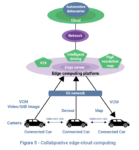
Edge computing technology will thus provide an end-to-end system architecture framework used to distribute computation processes to localized networks. A well-designed AI self-driving and connected car will be a collaborative edge-cloud computing system, efficient video/image processing, and multi-layer distributed (5G) network – a mixture of localized and cloud processing. Edge AI computing is meant to complement the cloud, not completely replace it.

Speed
Given the massive volume of data transmitting back-and-forth over a network, for safety reasons, much of the processing has to occur onboard the vehicle. The speed at which the vehicle needs to compute continuous data, without the need to transfer data, will help reduce latency and increase accuracy due to a reliance on connectivity and data transfer speeds.

The interdependency between humans and machines means the velocity of information transfer in real-time is essential. Using edge AI computing involves having enough localized computational processing and memory capacities to be able to ensure that the self-driving car and the AI processor can perform their needed tasks.

Reliability
The safety of autonomous cars is critical. Edge computing reduces the strain on clogged cloud networks and provides better reliability by reducing the lag between data processing and the vehicle. It didn’t take long for autonomous vehicle manufacturers to realize the limitations of the cloud. While the cloud is a necessity, autonomous cars require a more decentralized approach.

With edge computing and edge data centers positioned closer to vehicles, there is less chance of a network problem in a distant location affecting the local vehicles. Even in the event of a nearby data center outage, onboard intelligent edge inferencing of autonomous vehicles will continue to operate effectively on their own because they handle vital processing functions natively.

Today, automakers provide multiple layers of protection and redundancy for power failure, network failure and even compute failure. Vehicles also have the ability to dynamically re-route and power network traffic and even decision-making to bring an autonomous car to a safe stop. Driverless cars with edge AI computing can support onboard diagnostics with predictive analytics, a system that can grow and evolve in features over its lifecycle.

With so many edge computing vehicles connected to the network, data can be rerouted through multiple pathways to ensure vehicles retain access to the information they need. Effectively incorporating Internet of Vehicles (IoV) and edge computing into a comprehensive distributed edge architecture providing unparalleled reliability and availability.

Security
The ultimate challenge of designing an edge computing ecosystem for autonomous vehicles is to deliver enough computing power, redundancy, and security to guarantee the safety of autonomous vehicles. Thus, protecting autonomous driving

edge computing systems against attacks at different layers of the sensing and computing stack is of paramount concern.

Security of autonomous vehicles should cover different layers of the autonomous driving edge computing stack. These securities include sensor security, operating system security, control system security, and communication security.

In addition, AI at edge gateways reduces communication overhead and less communication results in an increase in data security.

Scalability
Vehicular edge computing inherently has a distributed architecture that can help bring data to the edge of networks, where vehicles can analyze and interact with the data in real time, as if it were local.

While the cloud is a necessity for certain tasks, autonomous cars require a more decentralized approach. For example, intelligent sensors can have the capability to analyze their own video feeds, determine which frames of a video require attention and send only that data to the server. This decentralized architecture reduces network latency during the data transfer process as data no longer has to traverse across the network to the cloud for immediate processing. AI vehicles are being equipped with more onboard computing power than in the past and can perform more tasks on their own. with higher predictability and less latency.

Cost
The increasing number of roadside units (RSUs) equipped with powerful local AI processors can help lower energy consumption, maintenance and operational costs as well as the associated high bandwidth cost of transferring data to the cloud. Meanwhile, one of the key drivers making edge computing a more viable reality today is that the cost of computing and sensors continues to plunge.

AI Automotive Processor Technology
The automotive industry is undergoing key technological transformations, advancing towards higher automation levels. Intelligent driving requires more efficient and powerful AI processors. According to Horizon Robotics’ summary of OEM demands, a higher level of automated driving requires more orders of magnitude tera operations per second (TOPS), namely, 2 TOPS for L2 autonomy, 24 TOPS for L3, 320 TOPS for L4 and 4,000+TOPS for L5.

Automotive processors typically fall into three broad categories:

  1. CPU and GPU-based processors: tend to have good flexibility but generally consume more power
  2. FPGAsrequires less computational resources, but more costly and limited programmability compared to GPUs
  3. ASICs: usually with a custom design, are more efficient in terms of performance, cost and power consumption

Conventional CPUs and GPUs are struggling to meet the increasing demands of high computing requirements of L4 and L5 autonomous driving levels where FPGAs/ASICs are both outperforming CPUs/GPUs. Autonomous vehicles will need enough

computing power to become a “data center on wheels”. Taking the complexity of automotive applications into consideration, computing power alone is not enough. The energy efficiency, performance and cost-effectiveness of AI automotive processors should also be taken into consideration. Full-custom ASICs are by far superior to GPUs/FPGAs in terms of lower power consumption, performance and cost. That is why the integration of AI-specific ASIC accelerators in autonomous driving computing platforms is booming.

High-Performing Accelerator Chips
The inference accelerator chips of Gyrfalcon Technology, Inc (GTI) have a Convolutional Neural Network Domain-Specific Architecture (CNN-DSA) with a dedicated Matrix Processing Engine (MPE) and an efficient AI Processing in Memory (APiM) technology. As an example, GTI’s LightSpeeur 2803S provides a power efficiency performance of 24 TOPS/Watt with all CNN processing done in the internal memory instead of outside DRAM. It can classify 448×448 RGB image inputs at more than 16.8TOPS with a peak power consumption of less than 700mW and with an accuracy comparable to the VGG benchmark. Gyrfalcon’s CNN- DSA accelerators are reconfigurable to support CNN model coefficients of various layer sizes and layer types.

For more computationally-intensive edge computing applications such as in driverless-car AI platforms, GTI’s PCIe- based AI accelerator cards using 16x 2803S chips delivering 270 TOPS and 9.9 TOPS/W power efficiency can be used for Level 4 AI auto performance demand. Using 4x GTI 2803S PCIe cards (64 chips) can provide the top performance of 1080 TOPS for L5 AI auto performance and beyond.

GTI’s AI-based chips have a flexible and scalable architecture and can be easily arranged in either parallel or cascades for any given performance/model size application. Cascading capability provides flexibility and reduces the host workload. Cascading enables support for larger and more complex models (i.e. ResNet-101, ResNet-152, …).

The underlying function of many autonomous vehicle applications is deep-learning technology, such as convolutional neural networks (CNNs) that are typically used for vehicle and pedestrian detection, road surface tracking, sign and signal recognition, and voice-command interpretation. GTI’s AI-based architecture is “silicon-proven” standalone accelerator technology that can be used with any type of sensor output, such as visual, audio and other forms of data. This can include high data rates from machine learning cameras and high-resolution LiDAR as well as low data rates from RADAR and ultrasonic sensors.

About Manouchehr Rafie, Ph.D.
Dr. Rafie is the Vice President of Advanced Technologies at Gyrfalcon Technology Inc. (GTI), where he is driving the company’s advanced technologies in the convergence of deep learning, AI Edge computing, and visual data analysis. He is also serving as the co-chair of the emerging Video Coding for Machines (VCM) at MPEG-VCM standards.


Musk’s Massive Mobile Gambit

Musk’s Massive Mobile Gambit
by Roger C. Lanctot on 08-11-2021 at 10:00 am

Musks Massive Mobile Gambit

A few weeks ago Mobile World Congress included among its keynotes a live interview with Tesla CEO Elon Musk moderated by Mobile World Live Publisher Justin Springham. The subject was Starlink, the low earth orbit (LEO) constellation intended to deliver global Internet access.

Mobile World Congress Musk keynote interview

Tongue-in-cheek speculation has long suggested that Musk intends to bring satellite connectivity to Tesla automobiles with Starlink. Some commenters have taken to Photoshop to create silly pictures of Teslas outfitted with the ungainly Starlink antenna.

Musk has a far more cunning plan in mind, according to his interview. He revealed that he is in talks with multiple telecom companies which are seeking to solve their 5G rural coverage and backhaul challenges. Starlink might be the ideal solution for doing just that.

The idea ought to take the breath away from every executive responsible for automobile connectivity. A collaboration of this sort with wireless carriers solves some fundamental problems for those carriers and might convince them to give Tesla advantageous rates for connecting cars.

Carriers with expensive 5G licensees often have rural service delivery requirements to fulfill to put their licenses to work in deploying 5G. At the same time, telecommunication companies may put up towers in remote areas to fulfill those requirements, but will still require backhaul.

With his 1,600+ satellites in low earth orbit, Musk has a tantalizing solution to this regulatory problem. Providing this kind of service to wireless carriers with 5G licenses may give Musk an alternative path to positive cashflow.

Estimates are that when all is said and done, developing, launching, and completing the creation of the Starlink constellation will have cost the company $10B. Musk currently claims to have more than 10,000 customers paying $99/month for Internet service, after having installed their $499 Starlink antennas. Musk adds that the antennas are being sold at a loss. This kind of piddling revenue stream would put Starlink on the fast-track to bankruptcy – the usual path followed by satellite startups.

You don’t need to be a rocket scientist to see that Starlink will never recoup its $10B investment delivering satellite connectivity to mountaintop and rural users around the world – even if Starlink is able to reach the 500,000 subscribers that it foresees. Starlink might, however, recover that investment as an infrastructure play.

In fact, Musk may even be seeking to provide the solar power to support equipment located in rural or remote locations – often supported currently by diesel generators. Such a gambit fits with Musk’s pattern of leveraging government support.

Whether it is hundreds of millions of dollars in carbon credits or juicy SpaceX contracts with the Federal government to serve the International Space Station, Musk has consistently aligned his commercial objectives with publicly funded initiatives. Now, he is signing on to help solve the broadband-for-all agenda inherent in the soon-to-be-passed infrastructure legislation in the U.S.

Satellite connectivity is already widespread in cars including GPS and, in the U.S., SiriusXM – and more is coming. Starlink will not be part of that story. Musk’s collaboration with carriers, though, may give Tesla a leg up on advantageous wireless rates – maybe.


Debugging Embedded Software on Veloce

Debugging Embedded Software on Veloce
by Bernard Murphy on 08-11-2021 at 6:00 am

Debugging Embedded Software on Veloce min

Arm provides great support for debugging embedded software in its CoreSight tools, but what support do you have if you’re debugging hardware and software together in a pre-implementation design? In a hardware debugger you have lots of support for hardware views like waveforms and register states. But these aren’t well connected to what you expect in a software debugger – a source code view allowing for single-stepping, and visibility into variable and memory contents. Worse yet, since the software debugger follows emulation in the debug pipeline, the software can miss closely sequenced hardware events which may be critical to understanding a problem.

Fall back to assembly-level debug?

In my college days one of our lab projects required us to build a project with an early microprocessor, together with our own assembler. I have no idea why this was an option in our physics lab. In those days maybe this was considered more physics than engineering. Anyway, we built and demonstrated a DFT, cycling through lots of rounds of debug in testing the assembly code. That took a while even though our idea of debug was whether the output looked right given what we’d dialed on the signal generator (sine wave, square, etc). This was a very simple processor; even so it took us a while to get right. Proving to me that while it might be interesting to understand the primitive code that drives such a machine, I didn’t want to make a career of it.

Neither do most of us, especially now that processors are significantly more complex and come in clusters. But perhaps given the challenge I mentioned earlier, when you run into a bug you can’t figure out you might suffer temporary insanity. Perhaps, you tell yourself, I should give assembly-level debug a shot. Siemens recently published a white paper with a reminder of why you don’t want to follow this path.

They illustrate through the steps they must follow from a flatlined simulation. First to find the corresponding line in the assembly code. Then tracking that to the C-source code. Figuring out the call stack. Then figure out which variable might be at fault. And finally go back to the waveform view to realize that a pointer variable went to zero. All makes sense but that was a lot of steps to go through to find just the first problem. The first of many in what will likely be a much longer diagnostic search.

Better to couple hardware debug to a code debugger

Siemens offer Codelink to view and debug source code directly with Veloce. You’ll typically do this offline from emulation, since debug involves a lot of head-scratching and what-if-ing. You don’t want to tie up a premium resource while you’re doing that. With a full run-dump from Veloce, you don’t have to. In the example above, you can jump immediately to the last line executed in the source code, instantly understand the code stack and hover over any variable to get its value at that point. One the debug run has loaded you see in seconds that the pointer is zero and you can move on to figure out why.

Codelink has full support for Arm v8 and V9, and access to memory data, register values and disassembly. It also supports multi-core debug, correlation between source window actions and waveforms and power activity. Sure it’s not CoreSight, but CoreSight can’t look into all the other hardware you added to your SoC. Codelink covers both bases well enough to support your full SoC+software debug needs. You can read the Siemens white paper HERE.

Also Read:

SoC Vulnerabilities

A Custom Layout Environment for SOC Design Closure

Siemens Offers Insights into Gate Level CDC Analysis


The Quest for Bugs: “Shift-Left, Right?”

The Quest for Bugs: “Shift-Left, Right?”
by Bryan Dickman on 08-10-2021 at 10:00 am

Quest for Bugs Shift Left EDA

Shift-left, why?

Shift-left testing is an approach to software and system testing which is performed earlier in the lifecycle (that is, moved left on the project timeline). It is the first half of the “Test early and often” maxim that was coined by Larry Smith in 2001.

It’s now an established idea, much talked about in both software and hardware engineering as a philosophy to drive testing as far to the left as possible on the project timeline, thus, removing bugs earlier, when they are cheaper and faster to find, and the bug impact costs are much lower.

So, shift-left has the potential to magnify these cost savings by reducing the number of bugs that are propagated downstream only to be found and then fixed at a much later time when the rework costs may be much higher and associated failures cause serious risks to life, or function.

We are going to discuss shift-left in the context of using virtual prototyping at the front-end of the development lifecycle. We will explain how shift-left with virtual prototyping will find software bugs earlier, and also find hardware bugs earlier. In the “quest for bugs”, finding bugs earlier is a significant win for the developers and users of ASIC.

Shift-left, how?

Virtual Prototyping enables a shift-left of the overall product development time by allowing development of the system software and firmware in parallel, even ahead of the design RTL bring-up. The Virtual Prototype (VP) decouples the system software development (BIOS, firmware, device drivers), OS porting/development, and application software development, from the RTL hardware development. VP Kits are easy and inexpensive to deploy to both internal and 3rd party software developers. This shift-left of the software bring-up enables the software developers to flush out most of the software bugs ahead of the hardware development. It’s essentially frontloading the software bug quest. The following diagram illustrates the measurable benefits of this shift-left for software development. However, Virtual Prototypes fulfil several other demands that will reduce the overall effort for RTL verification. By eliminating most of the software bugs ahead of the point where software-driven verification begins, the debug effort is significantly reduced, and the engineering effort can be focused on finding RTL bugs more efficiently.

Bringing up new hardware and new software/firmware together for the first time, leads to a double-blind situation which means debugging both in parallel – difficult!

Virtual prototyping enables a “find and fix” approach for most of the software/firmware bugs ahead of RTL verification. Further, the use of VP models in hybrid verification workflows (simulation, emulation and FPGA prototyping), reduces the mean-time to find bugs, by significantly accelerating these environments, especially when replacing a major RTL component such as a processor, with a fast VP model.

                                     Source – Acuerdo and Valytic Consulting

Better Software. Faster![1]      

In the above diagram, without Virtual Prototyping, System-software development (i.e. firmware/BIOS, RTOS porting, device drivers, and also possibly compilers and other software tools) is dependent on hardware development to provide a stable software execution environment. System-software developers will need to develop and validate code by running on either RTL emulation models, or FPGA prototypes. This presents a number of challenges in distribution, performance, and availability of the software execution environment. As mentioned in “System Bug Quest” and “Deep Cycles”, this can be accomplished with a centralized and scaled-out FPGA prototyping farm (or cluster).

This may be achievable for your internal software team (the system-software team), but what about internal or external Application-software developers, say for example an automotive company SW team developing a new autonomous driving chip? This community of software developers may need to wait for prototype silicon in the form of development boards, which can push application-software development far out to the right.

Earlier system-software        

When a VP Kit (VPK) is developed up-front, the system-software is decoupled from the RTL development and can be developed in parallel. Thus, we have a shift-left for the delivery of the system-software.

Earlier application-software 

Application-software is also decoupled from the HW development and is no longer dependent on the availability of hardware in the form of development boards. VPKs are easy to distribute to software development teams, since they are software tools. However, the application-software development still has a dependency on the availability of the system-software in most cases, especially for vertical end-to-end integration testing of the entire software stack.

DevOps enabler        

CI/CD (continuous integration/continuous delivery) is a standard best practice for modern software developers who are aligning to a DevOps approach. For the CI part, the cycle of build-test-merge can be enabled by a fast VP model, allowing fast regression testing of software code changes, as the gate-keeper for codebase repository commits. This continuous testing of the software ensures that bad commits are avoided, the codebase is “always-working” and software bugs are minimized even under high levels of code churn.

Better Hardware. Faster!      

Hardware tape-out is generally dependent on completion of software-driven system validation. This phase is normally performed on hardware acceleration platforms (emulators, or FPGA prototyping systems). Software-driven system validation (the clue is in the name), requires the software, so cannot begin until sufficient system-software is available as validation payloads.

A VPK enabled workflow yields several realisable benefits for the hardware development lifecycle.

Less bugs in the hardware/software interface        

Although additional investment is required for the VPK development, arguably the RTL development will be shorter as the hardware/software interface has been pre-validated and is no longer part of the RTL development process. Otherwise, the hardware-software dependencies might not be exposed until later in the system-software development phase, and this could lead to more impactful re-working of the hardware leading to an overall higher hardware development cost. Co-development of the hardware and system-software would allow such issues to be identified sooner and more easily absorbed.

Software is ready      

With a VPK based workflow, system-software arrives much earlier thus enabling a system validation shift-left and earlier tape-out. Since the system software has been pre-validated against the VPK, it will be more stable, and you avoid the double-blind debugging situation mentioned previously.

Verification shift-left 

VP models can be used to shift-left the development of RTL testbench environments thanks to co-simulation. For example, the VP can be used as a “Virtual-DUT” so that testbenches and test-cases can be developed, and verification bugs can be reduced in advance of RTL. Further, system-level test-cases can be developed in advance of RTL to speed up system integration testing.

“Accelerated acceleration”  

VP models written in SystemC/TLM can be mixed and matched with RTL components to build hybrid- emulation, or hybrid-FPGA-Prototyping environments. The VP components are simulated on the host workstation while the RTL components are mapped to the hardware acceleration platform. This can be done early on in the development lifecycle to enable prototype development in advance of RTL, or when building a VP model of the complete system where one or more components do not exist as VPs but RTL is available. Alternatively, it can be used to swap out larger off-the-shelf RTL components (e.g. processors) with fast VP models, leaving only the RTL-under-development to run on the hardware acceleration platform. For example, replacement of a processor RTL model with a processor cycle approximate VP model will speed up code execution runtimes by several orders of magnitude (e.g. OS boot). Further, a reduction in the footprint of the hardware accelerated RTL model may increase the hardware acceleration system clock speed (e.g. less FPGAs required to map the design, reduces design partitioning overhead and effect on clock speed), and free up hardware acceleration resources. Modern emulation and FPGA prototype systems are designed to connect to VP models through libraries of ‘transactors’. These transactors allow the efficient mapping of virtual I/O transactions onto the pin-level activity of the RTL model.  They are abstraction-level converters.

These benefits for hardware acceleration yield a further shift-left effect for the software-driven system validation phase of hardware development.

                                     Source – Acuerdo and Valytic Consulting

Power validation feed-forward        

When your virtual prototyping environment supports power exploration, these findings can be used to feed-forward into emulation power analysis workflows (see “Power Bug Quest” for more details).

Shift-left, right!

Recent reports show the global market for EDA Tools, estimated at US$10.5 Billion in the year 2020, is projected to reach a revised size of US$18.7 Billion by 2027[2]. Over a similar period, virtual prototyping is predicted to rapidly grow to a market size in excess of $860M by 2025[3]. It is perhaps surprising that this figure isn’t a larger proportion of tool spend, given the clear advantages it offers as a method to accelerate bug avoidance and avoid spending disproportionately more on other technologies, later in the design cycle.

Time to shift investment left?

In the semiconductor business the pressures of time to market and for products to be correct-by-design, the motivation is slightly different. Many companies have a verification philosophy that goes something like, “spend more on everything to avoid disappointment”. In other words, shift investment left to VP and “right” to emulation and FPGA simultaneously. However, not all companies can afford to do that, so it is well worth asking the “balance” question; what issues could we avoid by investing more in VP technology, as well as the necessary investments in emulation and FPGA and what are the likely returns?

While the most obvious and widely acknowledged advantage is the shift-left effect on software development, there are many other benefits that apply to hardware development with an overall multiplying effect on the final product delivery shift-left outcome!

Where do you and your team sit on the shift to virtual prototyping line…? 

References

[1] Although published in 2014, this book gives a very good overview of Virtual Prototyping use-cases and is still highly recommended.  https://www.synopsys.com/company/resources/synopsys-press/better-software-faster.html

[2] https://www.reportlinker.com/p05817912/Global-EDA-Tools-Industry.html

[3] https://www.grandviewresearch.com/industry-analysis/virtual-prototype-market


On-the-Fly Code Checking Catches Bugs Earlier

On-the-Fly Code Checking Catches Bugs Earlier
by Synopsys on 08-10-2021 at 6:00 am

Euclide GUI

There’s no question that chip designs are getting more complex, driven by the power, performance, and area (PPA) demands of applications like artificial intelligence (AI), automotive, and cloud computing. This complexity, of course, trickles down to the design and testbench code. When engineers can find and fix bugs before sending their code to downstream simulation, emulation, and implementation tools, that makes the whole design process that much more efficient.

How can you generate correct-by-construction code for a more productive chip design and verification process? Let’s explore how in this post, which was originally published on the “From Silicon to Software” blog.

While typing a document, functions like auto-correct and spell checking make it more efficient to generate a clean copy. What if writing SystemVerilog code for your chip design was just as efficient? As hardware description and hardware verification languages go, SystemVerilog is one of the most commonly used. However, it also happens to be an extraordinarily complex language, with RTL constructs, assertions, and support for object-oriented programming and constrained-random testbenches. Designers have to fully compile and elaborate their SystemVerilog code, allowing connection of all parts of their design and testbench and also enabling complex checks.

Much like the software development process, with RTL code for chip designs, it’s best from a time and cost perspective to address bugs before they become costlier and more time-consuming to fix later in the design process. In an ideal world, designers would catch as many types of problems as they can while entering their RTL. Verification engineers would do the same while coding their testbench. When teams are able to deliver correct-by-construction code, this is much like a shift left in the software world—and in this case, the resulting productivity lift accelerates the design and verification process.

Traditional Verification Can Be Labor Intensive

Traditionally, SystemVerilog or Universal Verification Methodology (UVM) testbench are only verified after handoff to simulation or emulation—a time-consuming and labor-intensive process. Sometimes, unoptimized testbench code in proprietary or off-the-shelf verification IP (VIP) can create performance bottlenecks for simulation. Similarly, RTL code is verified with linting or static verification tools after RTL handoff at the module level. However, sub-systems or SoCs are typically verified much later in the design cycle or overnight through lint regressions. The next day, the designer for each module would have to resolve the issues detected and run the tools again, repeating the process until all issues detected have been resolved. Further along the process, a synthesis, emulation, or static timing analysis tool could also catch issues. But by then, fixing those problems would involve many costly iterations. Plus, different tools in the design flow support different language-related constructs, and any syntax errors at a later stage could be very time consuming.

Another consideration is the increasing complexity of today’s chip designs, along with the fact that these designs are developed by teams that are typically distributed in different locations around the world. These trends have made RTL descriptions imperative for handling designs with millions or even billions of gates, while hardware verification languages are making sophisticated verification possible using testbenches with pseudo-randomized stimulus and self-checking of results. However, the process of integrating all of the RTL code modules—without error—can be a Herculean task. What if there are missing signals? What if there’s a missed connection at the sub-system or SoC level? Every aspect of the design must be explored, yet the modify-compile-run cycle for design and testbench code is a lengthy one that can get further stalled by even minor bugs.

The Keys to Writing Cleaner Code

What’s needed to write cleaner code—and to do it faster? A tool that works much like the auto-correct and spell-checking capabilities in word-processing programs. Ideally, such a tool would:

  • Perform full parsing of SystemVerilog code, down to the last parameter
  • Provide the parsing, compilation, elaboration, and synthesis while the user is typing in the code
  • Analyze signals at the bit level, detect dead code, and recognize clocks and resets
  • Suggest quick fixes for the user to consider applying as is or modifying before using
  • Be customizable to support a particular design or verification flow

To foster the on-the-fly code correction that can enhance design and verification productivity, the new Synopsys Euclide solution provides the capabilities we’ve just outlined. Built by RTL experts, the solution identifies complex design and testbench compliance checks during SystemVerilog and UVM development. Thanks to its advanced algorithms, the Synopsys Euclide solution fosters high-performance compilation, elaboration, and pseudo-synthesis to deliver real-time feedback to enhance design and testbench quality during code development. By comparison, with traditional flows, users have to wait up to an hour or longer after typing in their code before they’re alerted to any errors. Other tools typically notify users of only one or two errors at a time before needing to be run again, while the Euclide solution is quite resilient and can proceed forward with incomplete and even broken designs to report as many errors as possible. This error recoverability is unique and provides advanced feedback on incomplete code. Synopsys Euclide also has a very fast incremental compilation engine and is executed as the user types in code, providing almost instantaneous feedback.

This diagram displays the Synopsys Euclide architecture and GUI.

Watch the Synopsys Euclide solution in action in these two short videos. The first video highlights how the tool performs linting and cleaning of code from violations during coding.

[Will embed “Better RTL and Testbench Code with Synopsys Euclide” here]

The second video shows features including content assist, automatic code generation, semantic coloring, and the design hierarchy tree.

[Will embed “Coding Testbench & RTL Using Synopsys Euclide” here]

Getting the Most Out of Downstream Design Tools

The context-specific auto-completion and content assistance capabilities of the Synopsys Euclide tool are tuned for the Synopsys VCS® functional verification, Verdi® automated debug, and ZeBu® emulation solutions and are compatible with Synopsys RTL and design synthesis solutions. Because of this, Euclide can provide feedback on areas such as simulation performance, emulation, and synthesis compliance checks. In fact, any simulation, emulation, formal, or synthesis tool should compile much smoother if the design, assertions, coverage, or other testbench collateral have been developed with the Euclide solution.

To test-drive the tool, you can download a 30-day trial of the Synopsys Euclide solution.

In our Smart Everything world, chip designs will only continue to grow more complex to meet the needs of innovative applications that are changing how we live, work, and play. By identifying and resolving bugs in design and testbench code early, you can avoid unnecessary simulation or synthesis cycles, long debug sessions, and costly chip re-spins as you push to get your products to market swiftly.

By Alex Potapov, Distinguished Architect, and Kiran Vittal, Sr. Product Marketing Director; Verification Group, Synopsys

Also Read:

Upcoming Virtual Event: Designing a Time Interleaved ADC for 5G V2X Automotive Applications

Optimize RTL and Software with Fast Power Verification Results for Billion-Gate Designs

Driving PPA Optimization Across the Cubic Space of 3D IC Silicon Stacks


Executable Specifications Shorten Embedded System Development

Executable Specifications Shorten Embedded System Development
by Tom Simon on 08-09-2021 at 10:00 am

CATIA STIMULUS for Specifications

Even though AI is being used to replace procedural coding for many embedded applications, there is still, and will be for a long time, code that is written manually to deal with complicated inputs to control connected systems. Even in AI based systems there are programmer coded steps for responses to AI identified inputs. All of this code will start with specifications that are most often written in natural language form. Based on these written requirements testers will create test cases and developers will write code. According to Yves Génevaux, Sales Director for the STIMULUS product at Dassault Systèmes, there is a better way to develop embedded systems that start with executable specifications.

I spoke with Yves recently and he described the process they have used to help a large number of prominent corporations improve quality and reduce development and testing times. STIMULUS allows the creation of specifications in a way that resembles natural language but uses templates to create executable specifications. For instance, instead of writing “when the switch mode is OFF, headlights shall be ON”, the user creates a formalized requirement that reads “When   switch   is    ‘ON,     headlight   shall be   ‘OFF”. It is possible to nest executable templates and create Booleans as well. Inputs and outputs may also be defined as analog values.

CATIA STIMULUS for Specifications

Yves pointed out that many functional failures can be found to originate in faulty specifications, which is the last place developers tend to look during debug. Yves showed me how, with an executable specification, inconsistencies and errors can be found quickly in STIMULUS. This can change weeks of debug into an avoidable problem altogether. He cited one example where a major subway system supplier had spent weeks doing fruitless debug before they decided to employ STIMULUS. It took one day to rewrite the specification in STIMULUS, one day to find the conflicting requirements, and one week to rewrite the code and determine that is was compliant with its specification. This saved Millions of dollars in penalties for late contract delivery.

The benefits of an executable specification extend to developing test suites. The traditional method is for the test team to pick a set of requirements and write tests for them. More mistakes can be made here, and completeness is always difficult to obtain. It is always a struggle to get and quantify the level of test coverage for specifications. STIMULUS allows testers to automatically generate as many test cases as they like. These are run automatically, with the results available in a graphical interface. When there is hardware in the loop, STIMULUS performs automatic analysis of test log files to determine proper functionality.

Another example that Yves offered involved a tier one automobile supplier developing an emergency steering wheel function to take control in order to avoid an obstacle. The function was specified with 20 requirements. After using STIMULUS 12 conflicts were detected in the specification that had escaped notice previously. In addition, at least 8 more functional errors were discovered rapidly among the 20 requirements.

Yves was quick to point out that system complexity is not a major issue for STIMULUS. In larger systems each subsystem can be validated separately, then a set of subsystems can be validated as a whole and its behaviour compared to the upper level specification. This approach allows validating the specifications of very complex systems without any scalability issue.

STIMULUS represents a major shift in methodology that comes with big benefits. To help understand this Yves has created a library of videos that can be accessed on his LinkedIn profile. The clips that I reviewed showed the operation of STIMULUS and the tool set up. These videos can be found here on LinkedIn.

Also Read

Fully Modeling the Semiconductor Manufacturing Process

Optimizing high performance packages calls for multidisciplinary 3D modeling

A Brief History of IP Management


Quantum Computing and Threats to Secure Communication

Quantum Computing and Threats to Secure Communication
by Kalar Rajendiran on 08-09-2021 at 6:00 am

Our Panelists

There is never a dearth of new terms, discoveries and inventions in the technological world. And sometimes existing terms get reinvigorated. And debates ensue. The debaters argue about the plusses and minuses and make some predictions. Such is the case with “Quantum Computing.” I recently watched and listened to a webinar that provides insights into quantum computing, how advances in that field could pose a threat to secure communications and what is being done to address that threat.

The webinar was sponsored by Intrinsic ID, a leader in security IP for embedded systems based on physical unclonable function (PUF) technology. It was hosted on pufcafe.com. More on PUF Cafe later in this blog. The webinar was conducted as a panel session and moderated by Vincent van der Leest. The panelists were Dr. Pim Tuyls and Dr. Roel Maes. Pim is the CEO and Co-founder, Roel is the principal security architect and Vincent is the director of product marketing at Intrinsic ID. By the way, Intrinsic ID is a spinoff from Philips Research. Pim was one of the pioneers of PUF technology at Philips Research.

This blog is a summary of the salient points I gathered from the webinar panel session.

Before we dive into that, there are a few things to be clarified. For starters, the word “quantum.” In common parlance, it means quantity. But how much quantity? Generally speaking, people may think quantum means a lot, as in quantum improvement. Others may think quantum means instantaneous, thanks to the 1990s’ TV series Quantum Leap. But the theory behind quantum computing is quantum mechanics, the theory describing nature at the scale of sub-atomic participles. And quantum in this context means smallest possible discrete unit of any physical property such as energy or matter.

The other thing to recognize is that the term crypto as used in this webinar is shorthand for cryptography, not to be confused with crypto as in crypto currencies. Nor is this security topic limited to just crypto currency security but rather all kinds of secure communication applications. And this broad scope highlights the sense of urgency of the matter discussed in this webinar.

Quantum Computing

The promise of quantum computing is that it can deliver a level of compute performance that cannot be matched by today’s powerful computer chips. The performance results from tapping quantum phenomena such as superposition and entanglement to achieve computational parallelism.

Refer to figure below for comparing what can/can’t be done with classical computers vs quantum computers from the perspective of cryptography.

Quantum Computing Applications

At this time, there are a few known applications that could benefit from powerful quantum computing. In the field of computational chemistry, studying molecular interactions is a combinatorial problem with a very large search space. When we have powerful quantum computers, personalized drugs could be designed efficiently. Logistics is another field where problems could be solved very efficiently with quantum computing. There may be many more applications in the future.

Given the complexities involved in building quantum computers, it is fair to assume that it may take many years for us to see very powerful quantum computers. Pim says he expects it will take 10 to 20 years. So why this near-term concern about powerful quantum computers becoming a threat to secure communications?

A Few Reasons

Grover’s algorithm was invented in 1996 and uses brute force to deliver a performance at square-root of the search time of classical algorithms. It still takes exponential time but if the key used is not long, security could be compromised.

Shor’s algorithm was invented in 1994 and takes only polynomial time unlike Grover’s algorithm. So, increasing the key length does not have any impact. And this algorithm can break widely used security algorithms such as RSA, DH/DSA ECDH/ECDSA. Refer to figure below for what is worrying everyone.

And based on history, we know it takes a long time to upgrade all systems to start using newer security standards. For example, National Institute of Standards and Technology (NIST) established the Advanced Encryption Standard (AES) in 2001. From a practical perspective, the migration from Data Encryption Standard (DES) to AES has taken a long time. So, steps have to be taken now to develop and establish newer security standards that can stand attacks from quantum computers.

Post Quantum Crypto

NIST has been driving the initiative to develop and standardize security algorithms for the post quantum era. New algorithms can be expected to be finalized as early as next year and certainly within the next few years. To ensure smooth migration, playbooks should be written identifying who does what and where. For example, current silicon accelerators will stop working and would need to be redesigned.

PUF Technology

Because this is a webinar on pufcafe.com, Physical Unclonable Function (or PUF) technology is also discussed. Is PUF technology itself at risk due to quantum computing? The short answer is no. Pim explains how PUFs are quantum proof. But the keys could be at risk if used with RSA and other algorithms identified earlier.

PUF Cafe

For full details, please register at pufcafe.com and watch the entire webinar panel session. I certainly learned a lot. PUF Cafe is a great virtual watering hole to quench one’s thirst for security related knowledge and to separate myths from facts. There are many interesting webinars at PUF Cafe archives. You may want to regularly visit the site as they host webinars on interesting topics on a monthly basis.

Also Read:

Webinar: How to Protect Sensitive Data with Silicon Fingerprints

CEO Interview: Pim Tuyls of Intrinsic ID

IDT Invests in IoT Security