![]()
The 32nd VLSI Design/CAD Symposium just occurred in a virtual setting. The theme of the event this year was “ICs Powering Smart Life Innovation”. There were many excellent presentations across analog & RF, EDA & testing, digital & system, and emerging technology. There were also some excellent keynotes, and this is where I’d like to focus. TSMC’s Suk Lee presented a keynote entitled, “Moore’s Law and the Fourth Era of Semi”. Anything that attempts to make sense out of the storied and turbulent history of the semiconductor industry catches my attention. As explained by TSMC, the fourth era of semiconductor is all about collaboration. Let’s a take a closer look.
The keynote was presented by Suk Lee, vice president, Design Technology Platform at TSMC. I’ve known Suk for a long time, so this presentation was a must-see for me. I sold to Suk when I was at Zycad and he was at LSI Logic. That was challenging as Suk is not easily impressed. I then worked with Suk at Cadence where we achieved some great results. His high bar for technical excellence was alive and well and it helped us. Since Cadence, I’ve had a few gigs in companies that were part of the Design Technology Platform Suk oversees at TSMC. Again, meeting his high bar for technical excellence made us all better. Let’s look at the history of the semiconductor industry, according to TSMC and Suk Lee.
The First Era of Semiconductor – IDM
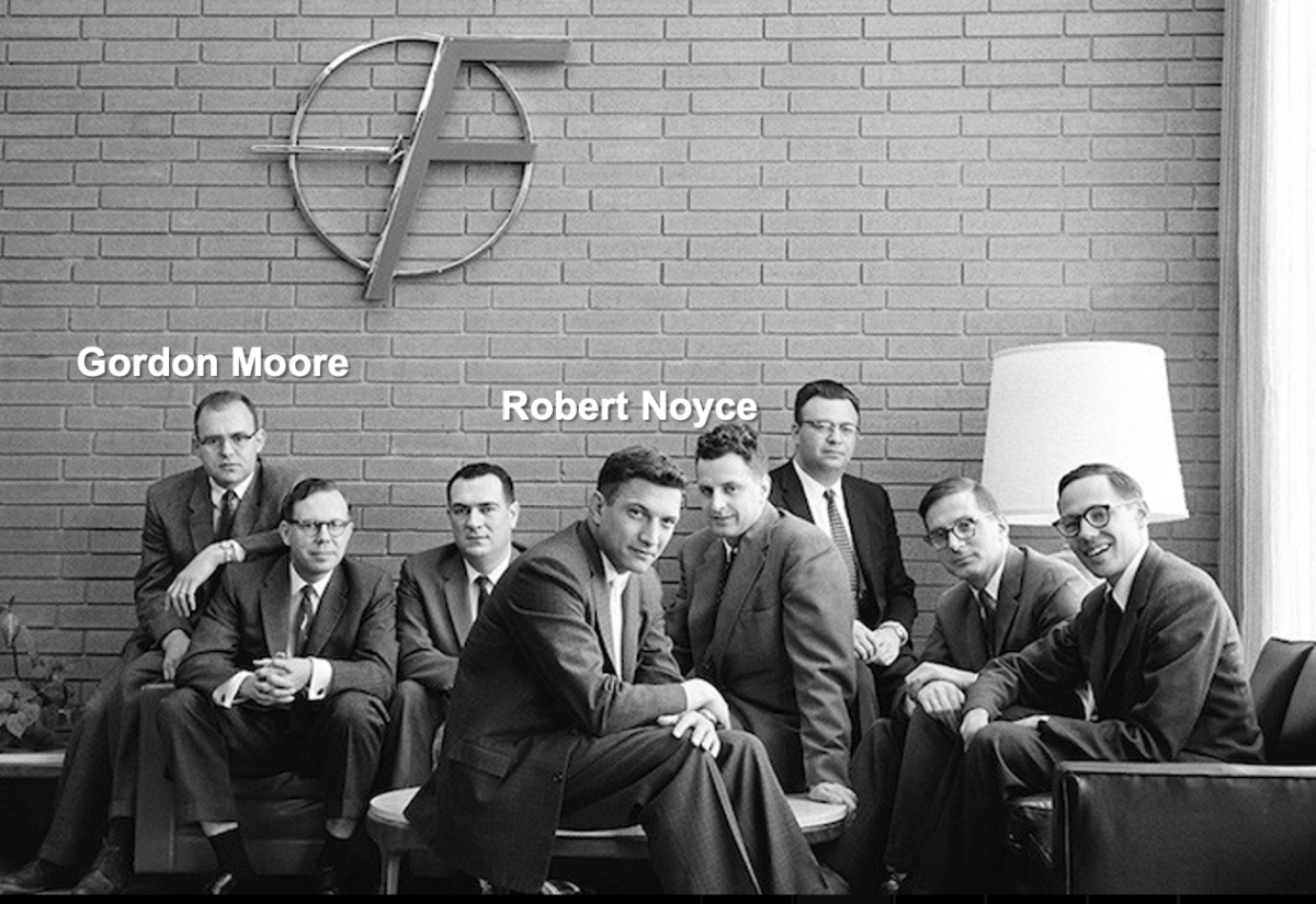
To begin with, the transistor was invented at Bells Labs, followed by the first integrated circuit at Texas Instruments. Things got really interesting when the first monolithic integrated circuit was developed at Fairchild. The photo below, courtesy of the Computer History Museum shows some of the early pioneers involved in this work. You will recognize their names. Note everyone is wearing a jacket and tie. This might be something to think about as you plan your return to the office.

And so, the first era of semiconductor was born – the Era of the integrated device manufacturer, or IDM. These were monolithic companies that did it all – chip design, design infrastructure, chip implementation and process technology. I started my career in the design infrastructure area at an IDM called RCA. Suk points out that integration and invention went hand-in-hand at IDMs. The opportunity to create something completely new was quite exciting. I know that from first-hand experience. Custom chips were the domain of IDMs. They had all the infrastructure, technology and staff to get it done. And so custom chips were limited to IDMs or companies with enough money to fund the massive development at an IDM. That all changed when we got to the second era of semiconductor.
The Second Era of Semiconductor – ASIC
Companies like LSI Logic and VLSI Technology were the pioneers for this phase. Now, design infrastructure, chip implementation and process technology were provided to all by the ASIC vendor. The semiconductor industry began to disaggregate during this time. Armed with design constraints, a much broader community of engineers could design and build a custom chip. The technology became democratized, and the world was never the same.
The Third Era of Semiconductor – Foundry
The third era is essentially a maturation of the second era. All of the steps in IC design and fabrication are quite challenging. Assembling an ecosystem where each company focuses on their core competence is a great way to manage complexity. This is what happened in the third era. Chip design and implementation were addressed by fabless semiconductor companies, design infrastructure was delivered by EDA companies and process technology was developed and delivered by foundries. TSMC was a key pioneer for this phase.
The Fourth Era of Semiconductor – Open Innovation Platform
Watch carefully, we’re about to come full circle. As the semiconductor industry continued to mature, process complexity and design complexity began to explode. Esoteric and subtle interactions between process technology, EDA, IP and design methodology became quite challenging to coordinate with a disaggregated supply chain. TSMC was the pioneer for this era as well.
The company realized that a substantial amount of coordination and communication was needed between the various parts of the disaggregated ecosystem. A way to bring the various pieces closer together to foster better collaboration was needed. And so, TSMC developed the Open Innovation Platform®, or OIP. They began this work early, when 65 nm was cutting edge. Today, OIP is a robust and vibrant ecosystem.
The infrastructure provided by TSMC paved the way for improved collaboration and coordination, creating a virtual IDM among its members. This provides TSMC’s customers the best of both the monolithic and disaggregated models. It changed the trajectory of the semiconductor industry and provided TSMC with a substantial competitive edge.
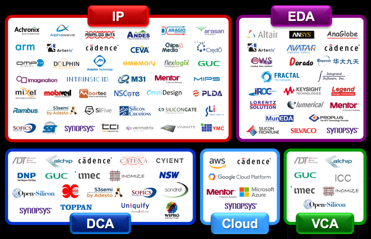
There are many benefits of the model. The ability to perform design technology co-optimization (DTCO) is one that is quite useful. The figure below illustrates the breadth of TSMC’s OIP. Advanced semiconductor technology requires a village, a big village. To help decode some of the acronyms DCA stands for design center alliance and VCA stands for value chain aggregator.

We’ve now reached the end of the semiconductor history lesson, for now. Getting to this point has been quite challenging and exciting. Suk Lee did a great job explaining the history. TSMC made it happen and we’re better as a result. I look forward the next phase of semiconductor growth and where it may take us. For now, remember that the fourth era of semiconductor is all about collaboration.
Share this post via:


Comments
One Reply to “TSMC Explains the Fourth Era of Semiconductor – It’s All About Collaboration”
You must register or log in to view/post comments.