RVN! 26 Banner revised (800 x 100 px) (600 x 100 px)

Synopsys Expands into Silicon Lifecycle Management

Synopsys Expands into Silicon Lifecycle Management
by Daniel Payne on 11-18-2021 at 10:00 am

SLM, Synopsys

I spoke with Steve Pateras of Synopsys last week to better understand what was happening with their Silicon Lifecycle Management vision, and I was reminded of a Forbes article from last year: Never Heard of Silicon Lifecycle Management? Join the Club. At least two major EDA vendors are now using the relatively new acronym SLM, and Synopsys defines it this way:

Silicon Lifecycle Management (SLM) is a relatively new process associated with the monitoring, analysis and optimization of semiconductor devices as they are designed, manufactured, tested and deployed in end user systems.

I had followed Moortec for a few years, and knew that Synopsys acquired this company for their embedded PVT sensors in November 2020. The second part of SLM is then to gather and analyze silicon data throughout the entire lifespan, so that even when the chips are running in a system you can analyze and even optimize the operation of your system.

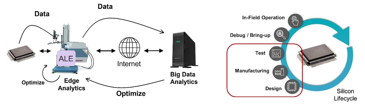
Another strategic acquisition that Synopsys made to start building up its SLM vision was Qualtera back in June 2020, and they provide big data analytics for semiconductor test and manufacturing. The early tools in SLM are well-known to IC design and test engineers, because they include DFT and ATPG. The later tools in SLM are the analytics and in-field optimization.  This is precisely where the latest acquisition of Concertio comes in, because they provide AI-based optimization of a running system. Here’s a graphical flow of the SLM vision, so that you can see all of the areas that it applies to:

Specific IP and EDA tools included within SLM, include:

  • DesignWare PVT monitors
  • Fusion Design Platform – placement of PVT monitors
  • SiliconDash – data analytics for semiconductor manufacturing
  • YieldExplorer – design centric yield management
  • SiliconMax high-speed access IP, TestMAX Adaptive Learning Engine

For in-field operations, the idea is to observer the software running on the system, analyze it, then tune the system. One example that comes to mind is how a vertically integrated company like Apple have optimized how their MacBook Pro laptop  has it’s battery charged to optimize it’s lifespan, because they know how often each app is run, what the power and RAM use for an app is, and can then control clock speeds based on workloads, control the RPM rate of fans and ultimately extend the lifetime of the battery.

Concertio is being used by systems companies to monitor work loads, optimize the compute resources through firmware settings, OS setting and even app settings, or Kubernetes settings on cloud apps. They use reinforcement learning in their AI approach for continuous, realtime optimizations. Users of Concertio technology are reporting improvements in the range of 5-15%.

From a marketing perspective, the SLM tools fall under the platform name SiliconMAX. I learned that the Concertio company was incorporated in New York, while their R&D team is in Israel, and they serve multiple markets, like: Cloud, on-premise compute centers, silicon design, high frequency trading. Synopsys has a good record of treating acquired companies quite well, and you can still visit the concertio.com web site, as they support customers and grow their business.

I could see some similarities in the approaches between the DSO.ai technology and what Concertio offers, as they both use reinforcement learning, so it will be interesting to see what kind of synergy there may be in the future. Stay tuned for more news as Synopsys integrates Concertio technology so that PVT analytics are fed into the system optimization loop, keeping SoCs running reliably.

Related Blogs


A Flexible and Efficient Edge-AI Solution Using InferX X1 and InferX SDK

A Flexible and Efficient Edge-AI Solution Using InferX X1 and InferX SDK
by Kalar Rajendiran on 11-18-2021 at 6:00 am

15 Transformer vs Traditional CNN 2

The Linley Group held its Fall Processor Conference 2021 last week. There were several informative talks from various companies updating the audience on the latest research and development work happening in the industry. The presentations were categorized as per their focus, under eight different sessions. The sessions topics were, Applying Programmable Logic to AI Inference, SoC Design, Edge-AI Software, High-Performance Processors, Low-Power Sensing & AI, Server Acceleration, Edge-AI Processing, High-Performance Processor Design.

Edge-AI processing has been garnering a lot of attention over the recent years and accelerators are being designed-in for this important function. Flex Logix, Inc, delivered a couple of presentations at the conference. The talk titled “A  Flexible Yet Powerful Approach to Evolving Edge AI Workloads,” was given by Cheng Wang, their Sr.VP Software Architecture Engineering. This presentation covered details of their InferX X1 hardware, designed to support evolving learning models, higher throughput and lower training requirements. The other talk titled “Real-time Embedded Vision Solutions with the InferX SDK,” was given by  Jeremy Roberson, their Technical Director and AI Inference Software Architect. This presentation covered details of their software development kit (SDK) that makes it easy for customers to design an accelerator solution for Edge-AI applications. The following is an integrated summary of what I gathered from the two presentations.

Market Needs and Product Requirements

As fast as the market for edge processing is growing, the performance, power and cost requirements of these applications are also getting increasingly demanding. And AI adoption is pushing processing requirement more toward data manipulation rather than general purpose computing. Hardware accelerator solutions are being sought after to meet the needs of a growing number of consumer and commercial applications. While an ASIC-based accelerator solution is efficient from a performance and power perspective, it doesn’t offer the flexibility to address the changing needs of an application. A CPU or GPU based accelerator solution is flexible but not efficient in terms of performance, power and cost efficiencies. A solution that is both efficient and flexible will be a good fit for edge-AI processing applications.

The Flex Logix InferX™ X1 Chip

The InferX X1 chip is an accelerator/co-processor for the host processor. It is based on a dynamic Tensor processing approach. The Tensor array and datapath are programmed via a standard AI model paradigm described using TensorFlow. The hardware path is reconfigured and optimized for each layer of AI model processing. As a layer completes processing, the next layer configuration is reconfigured in microseconds. This allows efficiencies approaching what can be expected from a full custom ASIC at the same time providing the flexibility to accommodate new AI models.  This reconfigurable hardware approach makes it well suited for executing new neural network model types.

A Transformer is a new type of neural network architecture that is gaining adoption due to better efficiencies and accuracies for certain edge applications. But transformer’s computational complexity far exceeds what host processors can handle. Transformers also have a very different memory access pattern than CNNs. The flexibility of the InferX technology can handle this.  ASICs and other approaches (MPP for example) may not be able to easily support the memory access requirements of transformers. X1 can also help implement more complex transformers efficiently in exchange for simpler neural network backbone.

The InferX X1 chip includes a huge bank of multiply accumulate units (MACs) that do the neural math very efficiently. The hardware blocks are threaded together using configurable logic which is what delivers the flexibility. The chip has 8MB of internal memory, so performance is not impacted due to being external memory-bound. Very large network models can be run off of external memories.

Current Focus for Flex Logix

Although the InferX X1 can handle text input, audio input and generic data input, Flex Logix is currently focused on embedded vision market segments. Embedded vision applications are proliferating across multiple industries.

The InferX SDK

The SDK is responsible for compiling the model and enabling inference on the X1 Inference Accelerator.

How the Compiler Works

The compiler traverses the neural network layer by layer and optimizes each operator by mapping to the right hardware on X1. It converts TensorFlow graph model to dynamic InferX hardware instances. It automatically selects memory blocks and the 1D-TPU (MACs) and connects these blocks and other functions such as non-linearity and activation functions. And it finally adds and configures the output memory blocks for receiving the inference results.

Minimal effort is required to go from Model to Inference results. The customer supplies just a TFLite/ONNX model as input to the compiler. The compiler converts the model into a bit file for runtime processing of the customer’s data stream on the X1 hardware.

Runtime

API calls to the InferX X1 are made from the runtime environment. The API is architected to be able to handle the entire runtime specification with just a few API calls. The function call names are self-explanatory. This makes it easy and intuitive to implement.

Assuring High Quality

Each convolution operator has to be optimized differently as that depends on the channel depth. Flex Logix engages the hardware, software and apps team to rigorously test the usual as well as the corner cases. This is the diligent process they use to confirm that both the performance and functionality of the operators are met. Flex Logix has also quantized image de-noising and object detection models and verified a less than 0.1% accuracy loss in exchange for huge benefits in memory requirement.

Summary

Customers can implement their accelerator/inference solutions based on the InferX X1 chip. The InferX SDK makes it easy to implement edge acceleration solutions. Customers can optimize the solutions around their specific use cases in the embedded vision market segments.  The compiler ensures maximum performance with minimal user intervention. The InferX Runtime API is streamlined for ease-of-use. The end result is CPU/GPU kind of flexibility with ASIC kind of performance at low-power. Because of the reconfigurability, the solution is future-proofed for handling newer learning models.

Cheng’s and Jeremy’s presentations can be downloaded from here. [Session 2 and Session 10]


Podcast EP49: Where Semifore fits in the design flow

Podcast EP49: Where Semifore fits in the design flow
by Daniel Nenni on 11-17-2021 at 10:00 am

Dan and Mike are joined by Rich Weber, co-founder and CEO of Semifore. Rich describes what the hardware/software interface is, where it fits in the design flow and the importance of a well-documented and robust design. He touches on industry standards, where they help and how Semifore’s products complete the flow. RIch also addresses what comes next with Semifore’s development.

https://semifore.com/

The views, thoughts, and opinions expressed in these podcasts belong solely to the speaker, and not to the speaker’s employer, organization, committee or any other group or individual.


Register Management is the Foundation of Every Chip

Register Management is the Foundation of Every Chip
by Mike Gianfagna on 11-17-2021 at 6:00 am

Register Management is the Foundation of Every Chip

Virtually every chip today runs software. And that software needs to interact with and control the hardware on the chip. There are typically many interfaces to manage as well as dedicated hardware accelerators to coordinate. In fact, many of those hardware accelerators are present only to support the execution of the software in a specific way. Most AI algorithms work like this. If you’re a software engineer, you will recognize the need for device drivers to accomplish these tasks. If you’re an architect, you know the register map is what makes the device drivers work. Managing those registers is a complex task and Semifore has a great white paper that explains the moving parts of this process. Read on to see why register management is the foundation of every chip.

The HSI

The register map implements something often called the hardware/software interface, or HSI. It’s the critical part of the design that ensures the device drivers can do what they’re supposed to. Getting the details of this part of the design correct, at the beginning is an important part of a successful project. It doesn’t end there, however.  A complex HSI can have millions of 64-bit registers. During design, bits in those registers can change quite often, many times per day. That necessitates creating a new version of the HSI and all the supporting documentation that often as well.  A methodology with substantial automation is the only way forward in this situation.

Where Semifore Fits

Semifore focuses exclusively on addressing the development of a verified, correct-by-construction HSI and propagating all the required formats to the various members of the design team. Ensuring everyone on the team is using consistent, up-to-date information is a critical item for smooth execution. Team members that need a unique format describing the HSI include RTL designers, verification engineers, software engineers and documentation staff. You can learn more about Semifore in this interview with Rich Weber, Semifore’s co-founder and CEO.

The White Paper

The Semifore white paper provides a great overview of the challenges of building the HSI and details that methodology with substantial automation I previously mentioned. The benefits of such a methodology are outlined in the white paper, as well as the pitfalls of trying to do it yourself.

A product design cycle is detailed to help you understand how the methodology fits. Aspects covered include:

  • Product definition phase
  • Product implementation phase
  • RTL verification
  • Software development
  • Documentation

Each section includes a detailed look at best practices and the benefits of following those practices. This document summarizes many years of experience Semifore has logged helping customers design highly complex chips. Reading it will save you a lot of time. You can access the white paper here.

One of the very challenging aspects of the HSI is managing all the objects and parameters that define its structure and behavior. There are industry standards that address part of this problem. There are also aspects not covered by those standards. It turns out Semifore has a solution for this problem as well. They have developed a language that is part of its product offering that picks up where the standards leave off.

It’s a way to build a real executable specification of your design. As a bonus, here is a link to the document that explains all the formats that need to be tracked, and how to capture them. After reading these white papers, you will appreciate why register management is the foundation of every chip, and how to build a solid foundation.

Also Read:

Webinar: Semifore Offers Three Perspectives on System Design Challenges

CEO Interview: Rich Weber of Semifore, Inc.


Where is the Monument of the Silicon Glen?

Where is the Monument of the Silicon Glen?
by Asen Asenov on 11-16-2021 at 10:00 am

NEC Plant Livingston

In 1991, I arrived in Glasgow to become a lecturer in Glasgow University, attracted by the Silicon Glen – the heart of semiconductor manufacturing in Europe. Here are few facts:

  • The larges semiconductor plant in Europe at that time was the NEC DRAM manufacturing site in Livingstone. When I visited the plant, I was mesmerized by the robot cars carrying the wafer batches between the processing stations. The plant closed in 2001 at the time of the great semiconductor industry downturn.
  • The first Motorola MOS plant was built in East Kilbride. I used to take students from my semiconductor course to visit. Usually in the parking you would see 6-7 Porsches. The Motorola guys were testing their Porsche chip sets on the cars and all Motorola managers were driving Porsches. The plant closed in 2003 also due to the semiconductor downturn.
  • The National Semiconductor plant in Greenock was pioneering the bipolar and BiCMOS technology. It is the longest standing semiconductor manufacturing plant in Scotland – from 1971 until now. After a sale to Texas Instruments the plant now has new owners – Diodes securing 300 jobs.
  • Perhaps the most sustainable small scale semiconductor operation in Scotland is Semefab. Founded in 1986 it is still going, offering foundry services for MEMS, CMOS, Opto-CMOS, Linear IC, BiCMOS, ASIC and Discrete Semiconductor device technologies.

Although not exactly semiconductor manufacturing, I would like to mention the IBM electronic manufacturing site in Spango Valley Greenock which had over 5000 staff at its peak. Combined with National this was almost 8000 staff in Greenock.

The Alba Centre in Livingstone established in 2000 around the idea of CMOS IP development in Scotland with Cadence in its heart was the Swan Song of the Silicon Glen. As a Head of the Department of Electronics and Electrical Engineering at Glasgow University at that time I was involved in the delivery of an MSc course in chip design for the 2000 future employees of Cadence who never came.

The hard lesson is that due to the semiconductor market turbulence inward investments from the big multinationals cannot sustain semiconductor expertise and manufacturing in our country. If a certain level of the vital advanced semiconductor manufacturing is to be resurrected in the UK perhaps the government need to think about a new model. However, these days creating advanced semiconductor manufacturing from scratch is only possible in countries with waste resources like China. For the UK will be very important to join forces with Europe and US in this area to remain competitive.


Siemens EDA Automotive Insights, for Analysts

Siemens EDA Automotive Insights, for Analysts
by Bernard Murphy on 11-16-2021 at 6:00 am

Siemens auto electronics min

There is a classical approach to EDA marketing, and semiconductor marketing at times, which aims exclusively at technical customers and the businesspeople immediately around those experts. The style is understandable and necessary. Those folks are the direct influencers and buyers of the products we are promoting, so we must capture and hold their attention. But many times this focus also seems to be assumed sufficient. We only need to speak to domain experts because the subject matter is far too complex for anyone else to understand. Besides, many attempts have been made to popularize the value of what we do to the larger world – analysts, investors, governments, and consumers – with questionable success. Beyond facile media comparisons, the gulf between what we do and how it affects large markets appears too wide to bridge.

Why is it important to speak to a larger audience?

Business success isn’t determined solely by customers and by being better that the competition. For an extreme example, look at Intel, now leveraging US government enthusiasm for rebuilding domestic semiconductor fab capacity. There are more immediate examples for the rest of us semiconductor types.

When a customer plans a large commitment to a vendor, they don’t only work through a technical checklist. They want to understand business characteristics of the vendor – financial performance and stability to support a long-term commitment. They want to understand what analysts, the press and other customers think of vendor market directions and ability to innovate; are these aligned with the customer?

The same applies to a potential buyer – of your company. Or a company you want to buy. The bond markets too, if you want to raise money. And of course, it applies to your stock price. Investors want to find undervalued companies with lot of growth potential, not stuck-in-a-rut companies.

Wider audiences need a different message

These audiences have limited if any appetite for technical specs. They want to understand why what you do is important and your track record in delivering on commitments to big name customers. Convincing them that you are a hot company to watch, the kind of company they should enthusiastically recommend, requires a different kind of marketing. Messaging of this kind should talk primarily about your customers’ customers (auto OEMs) goals and what it takes to meet those goals. Only towards the end does the story get into what part (at a high level) you can play in helping them meet those goals.

This is the Hero’s Journey, of which I’m a huge fan. The larger marketing world beyond semiconductors is already on-board. If you want more detail from a semiconductor perspective, read the book. I’m very encouraged to see Siemens EDA producing white papers in this class. This shows to me that they are fully embracing the larger perspective of Siemens marketing. Recognizing that they need to speak to and influence a much more diverse group than their traditional engineer, architect and product manager audience. Good for them!

Verification and validation for advanced cars

Now I’ve spent most of this blog waxing lyrical on why Siemens is doing this (see?), I should spend a little on what the paper is about 😎.  The first ~50% of the paper is on what automakers are aiming to deliver in SAE level 3 and beyond. And the opportunities and challenges in delivering to those expectations. Great start. We don’t all have a common understanding here, especially since the ground keeps shifting on when this might happen. Setting the context is important – the Call to Adventure.

The next ~25% of the paper is on development and verification implications. In being able to model, verify and validate hardware in the loop with other components of the system. This is critically important for autonomy modeling and testing. Where digital twin analysis over millions, even billions of virtual miles is becoming unavoidable. This is the Ordeal auto OEMs already face.

The last ~25% of the paper introduces how Siemens can help through their PAVE360 platform. In Hero’s Journey terms, where you as their Mentor explain to your customer how your solution can help them achieve their goals.

Nice job! You can read the white paper HERE.

Also Read:

Tessent Streaming Scan Network Brings Hierarchical Scan Test into the Modern Age

Minimizing MCU Supply Chain Grief

Back to Basics in RTL Design Quality


Tessent Streaming Scan Network Brings Hierarchical Scan Test into the Modern Age

Tessent Streaming Scan Network Brings Hierarchical Scan Test into the Modern Age
by Tom Simon on 11-15-2021 at 10:00 am

Streaming Scan Network

Remember when you had to use dial up internet or parallel printer cables connected directly to the printer to print something? Well even if you don’t remember these things, you know that now there is a better way. Regrettably, the prevalent methods used for hierarchical Design for Test (DFT) still look at lot like this – SoC level DFT has not kept up with design scaling. Fortunately, Siemens EDA has developed an entirely new methodology for connecting core level scan to the top level. Let’s acknowledge that hierarchical scan was a huge step forward. But, accessing the cores has always been done with methods that look like a room full of telephone operators individually connecting calls.

Siemens has published an article titled “Tessent Streaming Scan Network: A no-compromise approach to DFT” that clearly lays out the problems endemic with implementing full chip test using core level scan and pin-mux connections. The paper describes the Streaming Scan Network (SSN) approach that they have developed to address these problems. Using the old pin-mux technique, chip designers have to plan up front how to efficiently use a limited number of chip-level pins to facilitate testing. Critical decisions have to be made early in the design phase and are difficult to change later in development. Even running identical blocks in parallel runs into limitations. Up front decisions have to be made about which sets of identical blocks can be run in parallel. Pipelining to each block must match, and the results need to come back serially, etc. Even here there is no free lunch. For most other types of blocks it is equally messy.

To highlight the limitations of the pin-mux approach, the Siemens paper discusses several other problems. Hardwired buses need to be the proper width and have to be routed in advance in anticipation of how patterns will be run later. Branches that have blocks with shorter scan chains will leave bandwidth wasted. The routing itself can be problematic, especially when block to block connections in the chip are only are made with abutment.

Streaming Scan Network used in a 6 core design

Tessent SSN solves the problems with the pin-mux scan approach, while at the same time adding flexibility and making test operations measurably more efficient. Each core is fitted with a Streaming Scan Host (SSH) which acts as a local intelligent controller. Each SSH has two external connections – an IJTAG 1687 interface for coordinating test activities and the parallel SSN data bus. The SSN bus, while parallel, is independent of the number or size of the scanned cores. Scan data is sent in packets. The scan data for each target block is completely abstracted from the SSN packets, which can be intermixed and carry scan data of any width. The result is that the SSN can operate at full capacity and unwrap the scan data where it is used to interface with the core’s internal scan chain.

Parallel testing of identical blocks is made easy with scan packet delivery in parallel, regardless of the location on the SSN. Tests can be run in parallel, and local results checking can flip a pass/fail bit for each instance. The bus can also help adjust for slower internal shift frequencies by sending faster packets that are narrower to keep in sync with these blocks. Having a packetized smart network for moving scan and test data anywhere on the chip means that test strategies can adapt to the specifics of the design, even after tapeout.

The article offers a lot more detail on the specifics and advantages of Siemens Streaming Scan Network. It certainly moves DFT from the age of modems and parallel printer cables into the modern age of broadband and networked printers. The full article is available on the Siemens website along with full product information on Streaming Scan Network.

Also Read:

Minimizing MCU Supply Chain Grief

Back to Basics in RTL Design Quality

APR Tool Gets a Speed Boost and Uses Less RAM


A MIPI CSI-2/MIPI D-PHY Solution for AI Edge Devices

A MIPI CSI-2/MIPI D-PHY Solution for AI Edge Devices
by Kalar Rajendiran on 11-15-2021 at 6:00 am

Tradeoffs Edge vs Cloud

In late September, the MIPI Alliance held their DevCon conference as a virtual event. There were several excellent presentations at the conference. One of those was titled “A MIPI CSI-2/MIPI D-PHY Solution for AI Edge Devices” by Ashraf Takla of Mixel. Looking at the daily volume of technology news about applications moving to the edge, one may be led to believe pretty much every application has move to the edge. Ashraf does a wonderful job of establishing how cloud and edge processing complement each other and why appropriate partitioning is important for achieving optimal system performance. He then proceeds to explain why MIPI interface is a great fit for AI edge devices. You can watch Mixel’s entire presentation at MIPI DevCon here.

While theoretically everything can be processed at the edge or in the cloud, certain functional requirements drive the edge vs cloud processing decisions. This blog includes salient points garnered from the Mixel presentation.

Requirements Favoring Edge processing decisions

  • Low latency in order to make decisions in real-time or near real-time
  • Minimizing false notifications to improve battery life; processing at the edge requires less bandwidth as well, enabling more power savings
  • Security and Privacy; reducing chances for security breach by minimizing/eliminating transmission of raw data to the cloud for processing
  • Local processing due to unavailability of broadband/mobile connectivity
  • Minimize connectivity costs by reducing bandwidth usage, even when connectivity is available

Requirements Favoring Cloud processing decisions

  • High-capacity compute performance not available at the Edge; essential for complex machine learning and modeling
  • Large storage capacity
  • Ability to scale storage and compute resources at incremental cost
  • High security of data in the data center (but at-risk during data transmission)
  • Ease of maintaining and upgrading the hardware

The following is a functional requirements tradeoff table that Mixel has pulled together comparing edge and cloud computing.

MIPI

In the world of electronics, interfaces abound. Whether it is interfaces between systems or between chips, they are based on standards. Standards ensure compatibility and interoperability. One such interface that has found wide adoption is MIPI. Originally, it was developed to standardize interfaces within the mobile phone industry. Not only has MIPI beaten out other competing standards, it has also expanded its use cases. It is used in many more applications than it was originally developed for. That is the reason the expanded form of the MIPI acronym is not used anymore. 

Why is MIPI Attractive for AI Edge Devices

While already among the popular interfaces, MIPI is seeing rapid demand growth from artificial intelligence (AI) driven surge in the marketplace. Whether it is for IoT applications or automotive applications, they all use lots of sensors to gather data to make AI-based decisions. This data needs to be processed to make real time decisions right there in the field. Because of this low latency requirement, cloud-datacenter based processing is giving way to AI edge processing.

Many AI edge applications have very low power and strict EMI requirements. At the same time, they also have reasonable bandwidth needs. MIPI is able to satisfy all three requirements. This expands the range of devices that are attracted to MIPI with many devices being battery-operated and worn/carried on a person.

Additional Points of Interest

During the presentation, Mixel also spotlighted an edge-AI processor that uses its MIPI D-PHY, built on Global Foundries 22FDX process. The Ergo inference processor from Mixel’s customer Perceive, can be used to make decisions at the edge. The talk covered use cases for this processor in various target applications. The performance aspects of this processor were covered in an earlier blog.

Ashraf also used one slide to summarize the rationale behind Perceive’s choice of a fully depleted silicon on insulator (FDSOI) process technology for implementing the Ergo SoC. This relates to prior work completed by Mixel that was published in EE Times and covered in an earlier blog.

Summary

The way a system is partitioned between what computing is done in the cloud and what is done on the edge device is important. This will help optimize the system performance and determine the viability and success of a particular product. AI edge devices use many types of sensing (visual and audio) to solve specific problems. MIPI specifications are designed from the ground up to enable low power, high bandwidth requirements of edge devices. The selection of process technology for implementing MIPI PHY and edge chips is an important decision.

If you would like to learn more information about Mixel and their MIPI offering, visit their website here or learn about their MIPI D-PHY IP here.

Also Read:

FD-SOI Offers Refreshing Performance and Flexibility for Mobile Applications

New Processor Helps Move Inference to the Edge

Mixel Makes Major Move on MIPI D-PHY v2.5


Revisiting EUV Lithography: Post-Blur Stochastic Distributions

Revisiting EUV Lithography: Post-Blur Stochastic Distributions
by Fred Chen on 11-14-2021 at 10:00 am

Revisiting EUV Lithography Post Blur Stochastic Distributions

In previous articles, I had looked at EUV stochastic behavior [1-2], primarily in terms of the low photon density resulting in shot noise, described by the Poisson distribution [3]. The role of blur to help combat the randomness of EUV photon absorption and secondary electron generation and migration was also recently considered [4-5]. However, up to now, blur resulting from electron and chemical species migrations had been given the classical continuum treatment, when in actuality, at the nanometer scale, we are again dealing with random numbers of discrete quanta, i.e., electrons or chemically reactive species. These discrete quanta still follow Poisson distributions [6]. So, it is necessary to have a stochastic reconsideration after blur has already been taken into account.

This reconsideration seems necessary after the latest results at 28 nm pitch were were reported at SPIE earlier this year [7]. In order to achieve better imaging, metal oxide resists were used. These have the benefit of higher EUV photon absorption, which should provide relief for stochastic behavior. Despite this advantage, stochastic aspects of the imaging remained severe. Higher doses in the range of 50 mJ/cm2 (~110 WPH on the NXE:3400C [8]) were required, but larger CDs or dummy subresolution assist features (SRAFs) were needed for larger pitches. With optimized illumination, printing a relatively isolated pair of 14 nm trenches separated by 14 nm (local 28 nm pitch) was impossible without stochastic defects and roughness. Therefore, the reconsideration of post-blur stochastic effects here will focus on 28 nm pitch.

Blur is practically limited to less than 5 nm (sigma) for 40 nm pitches or less [5]. Increasing blur would result in the distribution of quanta becoming flatter, and a generally worse image. There is a larger risk of stochastic fluctuations further from the edge (Figure 1).

Figure 1. Reactive species number distribution plotted vs. position. The species number is considered within a 0.84 nm x 5 nm strip, assuming 50 mJ/cm2 incident dose, 50% absorption, and 2 species released per absorbed photon. Left: 3 nm blur. Right: 7 nm blur.

A new consideration is the quantum yield (or quantum efficiency), i.e., how many quanta are released per absorbed photon. Quantum efficiency for EUV chemically amplified resists is around 2 [9,10]. To reduce blur to 2 nm or less, it is expected to limit this release, in order to avoid excess random secondary electron and reactive species migration [9]. In Figure 2, a 2X reduction in quantum yield for 2nm blur (compared to 3 nm blur) shows the risk of stochastic defects does not improve and could get worse. It should be no big surprise, as quantum yield reduction has the same final effect as reducing photon density. In all these cases, we see fluctuations that cross the threshold, which means both line bridging and line breaking defects are possible. Six sigma corresponds to ~1 ppb failure.

Figure 2. Reactive species number distribution plotted vs. position. The species number is considered within a 0.84 nm x 5 nm strip, assuming 50 mJ/cm2 incident dose, 50% absorption. Left: 2 nm blur, 1 species released per absorbed photon. Right: 3 nm blur, 2 species released per absorbed photon.

Moreover, line edge roughness can be studied by reducing the line section length being sampled. Going from 5 nm to 1 nm section length, even 3 sigma fluctuations cross the threshold (Figure 3), indicating that roughness on the 1 nm scale is still present.

Figure 3. Reactive species number distribution plotted vs. position. The species number is considered within a 0.84 nm x 1 nm strip, assuming 50 mJ/cm2 incident dose, 50% absorption. 3 nm blur is assumed.

The only manageable solution to these issues remains to increase the dose (Figure 4). Given that there is already a throughput hit at 50 mJ/cm2, EUV source power will continue to be a priority target. However, higher doses could lead to larger blur due to the long tail detected in electron attenuation length measurements [11,12].

Figure 4. Reactive species number distribution plotted vs. position. The species number is considered within a 0.84 nm x 5 nm strip, assuming 50% absorption, and 2 species released per absorbed photon. Left: 50 mJ/cm2 incident dose. Right: 100 mJ/cm2 incident dose. 3 nm blur is assumed.

References

[1] https://www.linkedin.com/pulse/euvs-stochastic-valley-death-frederick-chen/

[2] https://www.linkedin.com/pulse/photon-shot-noise-impact-line-end-placement-frederick-chen/

[3] https://en.wikipedia.org/wiki/Shot_noise

[4] https://www.linkedin.com/pulse/contrast-reduction-vs-photon-noise-euv-lithography-frederick-chen/

[5] https://www.linkedin.com/pulse/blur-wavelength-determines-resolution-advanced-nodes-frederick-chen/

[6] G. M. Gallatin, “Resist Blur and Line Edge Roughness,” Proc. SPIE 5754, 38 (2005).

[7] D. Xu et al., “EUV Single Patterning Exploration for Pitch 28 nm,” Proc. SPIE 11614, 116140Q (2021).

[8] https://www.linkedin.com/pulse/challenge-working-euv-doses-frederick-chen/

[9] http://euvlsymposium.lbl.gov/pdf/2007/RE-08-Gallatin.pdf

[10] https://www.jstage.jst.go.jp/article/photopolymer/32/1/32_161/_pdf

[11] https://escholarship.org/content/qt4t5908f6/qt4t5908f6.pdf?t=qd3uq5

[12] https://www.euvlitho.com/2019/P66.pdf

Related Lithography Posts


US Supply Chain Data Request Elicits a Range of Responses, from Tight-Lipped to Uptight

US Supply Chain Data Request Elicits a Range of Responses, from Tight-Lipped to Uptight
by Craig Addison on 11-14-2021 at 6:00 am

China TSMC Supply chain woes 2021

Chinese state-run media blames Taipei for allowing Taiwan Semiconductor Manufacturing Co to submit chip supply information to the US government. Photo: Shutterstock

TSMC drew the ire of Chinese state media last week after it complied with the US Department of Commerce request to submit supply chain data by the November 8 deadline.

The Chinese reports, which called it an act of “surrender” to US hegemony, were careful in laying blame on Taipei for caving in to Washington, rather than pointing fingers at TSMC itself.

Chinese state media commentators are experts in party propaganda, not semiconductors, so they could be excused for not knowing the obvious: TSMC didn’t become the world’s leading foundry by blabbing about what its customers are doing.

Separately, Reuters quoted TSMC saying that it did not disclose any detailed confidential customer information to the US.

TSMC was one of 23 entities, including ASE, Infineon, Micron and Philips, that provided supply chain data, with most chipmakers choosing to do so privately rather than publicly disclosing their data.

But there were some interesting nuggets to be found in the public submissions.

On the customer side, Philips revealed that it had to delay 13 per cent of its production due to the semiconductor shortage. It added that the most severe shortages were in MCUs, FPGAs, ASICs, memory, linear and discretes – and that sourcing hard-to-find components now takes 12 to 18 months compared to 3 months in normal times.

Technicolor was something you’d see on movie screens in the golden days of Hollywood. These days it is the trading name of a French based company (formerly Thomson) that provides, among other things, visual effects production services for movies. It also buys chips, but not anywhere near the quantity of a giant like Philips – and therein lies the problem.

As a small customer, Technicolor has little clout amid product shortages, and it expressed those frustrations in its submission.

“Technicolor’s IC supply chain visibility has been challenged and remains uncertain, with unstable raw material supply (lead-frame, substrate), shortages with IC fabs and OSAT balancing capacity (allocation) and material availability to prioritize supply impacting delivery schedules with the fluctuation in lead-time impacting delivery commitments,” the company said.

Rising costs from foundry suppliers like TSMC and UMC was another bone of contention for the French company.

“IC suppliers are requesting customers to pay expediting fees to secure supply from foundries, and logistic fees are ever rising from our freight forwarders.  Cost increases like this are not standard in the semiconductor market and go against Moore’s Law, which is why they were not foreseeable or expected.” Ouch!

Back on the chip supply side, Infineon was blunt in telling the US government what the “root cause” for the global chip shortage was: the JIT (just-in-time) manufacturing system.

“To really overcome the global chip shortage, the JIT system should be replaced by a collaborative platform where demand information is shared anonymously (to keep the competition going) but without the bullwhip bias,” Infineon said.

The bullwhip effect refers to the demand distortion that travels upstream in the supply chain, amplified by the lack of synchronization among supply chain members.

The most damning submission, though, came from the Institute for New Economic Thinking, which slammed member companies of the Semiconductor Industry Association (SIA) like Intel and Qualcomm for asking the US government for industry funding on the one hand, but using their spare cash for stock buybacks on the other. The latter, of course, is meant to boost share prices and increase the wealth of stock-holding executives at the companies.

“Most of the SIA corporate members now lobbying for the CHIPS for America Act have squandered past support that the US semiconductor industry has received from the US government for decades by using their corporate cash to do buybacks to boost their own companies’ stock prices,” report authors William Lazonick and Matt Hopkins charged.

“Among the SIA corporate signatories of the letter to President Biden, the five largest stock repurchasers – Intel, IBM, Qualcomm, Texas Instruments, and Broadcom – did a combined $249 billion in buybacks over the decade 2011-2020, equal to 71 percent of their profits and almost five times the subsidies over the next decade for which the SIA is lobbying.”

It’s not only chipmakers that do this. The Semiconductors in America Coalition (SIAC) was formed in May to lobby Congress for the passage of the CHIPS act. Members include Apple, Microsoft, Cisco and Google, who spent a combined $633 billion on buybacks during 2011-2020, according to the report, which pointed out this was about 12 times the proposed government subsidies under CHIPS to support wafer fabs on US soil.

“If the Congress wants to achieve the legislation’s stated purpose of promoting major new investments in semiconductors, it needs to deal with this paradox,” the report authors said.

Their suggestion: require the SIA and SIAC to extract pledges from members to end stock buybacks as open-market repurchases over the next 10 years.

Any bets on how the members will vote on that?

The Chip Warriors podcast series