RVN! 26 Banner revised (800 x 100 px) (600 x 100 px)

A Practical Approach to Better Thermal Analysis for Chip and Package

A Practical Approach to Better Thermal Analysis for Chip and Package
by Daniel Nenni on 12-13-2021 at 6:00 am

ANSYS Thermal Chip Model

Thermal modeling has become a hot topic for designers of today’s high-speed circuits and complex packages. This has led to the adoption of better and more sophisticated thermal modeling tools and flows as exemplified in this presentation by Micron at the IDEAS Digital Forum. The presentation is titled “Thermal Aware Memory Controller Design with Chip Package System Simulation” and covers the latest developments in both power modeling and thermal modeling by the Controller design team at Micron.

The first presenter is Shiva Shankar Padakanti, a senior physical design manager at Micron with over 17 years of experience in backend design and more than 33 tape-outs down to 7nm. Shiva introduces the two major thermal issues faced by his team: (a.) avoiding overly pessimistic thermal limits that degrade a chip’s performance, and (b.) avoiding thermal runaway – a reliability issue where local hotspots cause increased device leakage, which increases the temperature yet further.

Shiva sets the stage by discussing their traditional thermal analysis flow that assumed a uniform temperature across the entire chip based on total power and relied on simple power/temperature limits with a large safety margin. This constrained power signoff to use un-realistically pessimistic temperature limits because the analysis under-reported the true maximum temperature. This could lead to compromise in the design’s specification and significant loss in chip performance due to over-design. The first attempt to improve their analysis capability was to analyze the power on a block-by-block basis instead of full-chip. This gave a more realistic non-uniform temperature distribution but was still unable to account for temperature-dependent leakage power.

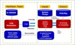
Working with Ansys, Micron developed a new analysis flow that uses the Chip Thermal Model (CTM) technology augmented with the APL Leakage Model. A CTM cuts each layer in the chip into a fine grid and then describes the power output of each grid square as a function of the temperature. The APL Leakage files capture how device leakage varies with temperature. These models are generated by Ansys RedHawk™ or Ansys Totem™ power integrity signoff and gives a much more accurate and fine-grained power model. This was then handed off to the Thermal team to enable their package and system thermal analysis.

Fig.1 Thermal analysis flow using Chip Thermal Models (CTM) generated by Ansys RedHawk or Ansys Totem power integrity signoff tools, and then used for package and system thermal analysis by Ansys Icepak.

The advantage of the CTM technology is that it accurately predicts the location of thermal hotpots and, in this test case, predicted a temperature 12% higher than the simpler block-based approach (see Fig.2). This higher temperature results from the accurate modeling of temperature-dependent leakage which was not considered in the block-based or traditional flows.

Fig.2 Shows a comparison of the temperature profile using the simpler block-based thermal modeling approach against the more accurate Chip Thermal Model that relies on a per-layer gridded model. The CTM technology accurately identifies the hotspot locations and predicts a 12% higher temperature based on temperature-dependent leakage

The second part of the presentation is narrated by Ravi Kumar, senior principal engineer at Micron with over 9 years’ experience  in thermal management of electronics. Ravi starts by pointing out that chip, package, and system analyses are each at a different scale – from microns to centimeters and thus require a range of simulation technologies to span this range. Also, simulating a complete stack as shown in Fig.3 is very computationally expensive for each temperature point, often limiting the scope of thermal analysis.

Fig.3 Cross section of the complete chip-package-system stack for the Micron controller under thermal analysis, including the PCB substrate and the external heat sink. The cooling airflow over the heatsink is modeled by Icepak using Ansys’ computational fluid dynamics technology.

However, by using the CTM modeling approach, Ravi’s team was able to speed up the thermal simulation time by 90% due to the higher efficiency and faster convergence of the CTM approach. The final operating temperature depends, of course, on its power output. But the power output is also temperature dependent. Icepak executes internal iterations using the CTM to arrive at a stable operating temperature. In this test case, the heat sink was designed to radiate an estimated 50W, but the system actually ended up generating closer to 60W. Failure to anticipate the real heat flow can heat stress the package and impact the performance and reliability of the entire system.

A final benefit highlighted by the Micron team was the ability to optimize the placement of thermal sensors on the chip. The traditional techniques had not accurately placed the sensors at the true maximum hotspots and under-measured the hotspot temperature by 8.1°C. The new CTM-based approach optimized their placement and reduced the risk of thermal runaway.

Shiva concluded the presentation by outlining future projects by his team to consider thermal-aware electromigration analysis, and the mechanical warpage of package and PCB due to thermal gradients.

You can view the entire Micron presentation on-demand at Ansys IDEAS Digital Forum under the Electrothermal Analysis track. Registration is free.

Also Read

Ansys CEO Ajei Gopal’s Keynote on 3D-IC at Samsung SAFE Forum

Ansys to Present Multiphysics Cloud Enablement with Microsoft Azure at DAC

Big Data Helps Boost PDN Sign Off Coverage


Edge Computing Paradigm

Edge Computing Paradigm
by Ahmed Banafa on 12-12-2021 at 6:00 am

Edge Computing Paradigm

Edge computing is a model in which data, processing and applications are concentrated in devices at the network rather than existing almost entirely in the cloud.

Edge Computing is a paradigm that extends Cloud Computing and services to the of the network, similar to Cloud, Edge provides data, compute, storage, and application services to end-users.

Edge Computing reduces service latency, and improves QoS (Quality of Service), resulting in superior user-experience. #Edge Computing supports emerging concept of Metaverse applications that demand real-time/predictable latency (industrial automation, transportation, networks of sensors and actuators). Edge Computing paradigm is well positioned for real time Big Data and real time analytics, it supports densely distributed data collection points, hence adding a fourth axis to the often-mentioned Big Data dimensions (volume, variety, and velocity).

Unlike traditional data centers, Edge devices are geographically distributed over heterogeneous platforms, spanning multiple management domains. That means data can be processed locally in smart devices rather than being sent to the cloud for processing.

Edge Computing Services cover:

  • Applications that require very low and predictable latency.
  • Geographically distributed applications
  • Fast mobile applications
  • Large-scale distributed control systems

Advantages of Edge computing

  • Bringing data close to the user. Instead of housing information at data center sites far from the end-point, the Edge aims to place the data close to the end-user.
  • Creating dense geographical distribution. First of all, big data and analytics can be done faster with better results. Second, administrators are able to support location-based mobility demands and not have to traverse the entire network. Third, these (Edge) systems would be created in such a way that real-time data analytics become a reality on a truly massive scale.
  • True support for mobility and the Metaverse. By controlling data at various points, Edge computing integrates core cloud services with those of a truly distributed data center platform. As more services are created to benefit the end-user, and Edge networks will become more prevalent.
  • Numerous verticals are ready to adopt. Many organizations are already adopting the concept of the Edge. Many different types of services aim to deliver rich content to the end-user. This spans IT shops, vendors, and entertainment companies as well.
  • Seamless integration with the cloud and other services. With Edge services, we’re able to enhance the cloud experience by isolating user data that needs to live on the Edge. From there, administrators are able to tie-in analytics, security, or other services directly into their cloud model.

Benefits of Edge Computing

  • Minimize latency
  • Conserve network bandwidth
  • Address security concerns at all level of the network
  • Operate reliably with quick decisions
  • Collect and secure wide range of data
  • Move data to the best place for processing
  • Lower expenses of using high computing power only when needed and less bandwidth
  • Better analysis and insights of local data

Real-Life Example:

A traffic light system in a major city is equipped with smart sensors. It is the day after the local team won a championship game and it’s the morning of the day of the big parade. A surge of traffic into the city is expected as revelers come to celebrate their team’s win. As the traffic builds, data are collected from individual traffic lights. The application developed by the city to adjust light patterns and timing is running on each edge device. The app automatically makes adjustments to light patterns in real time, at the edge, working around traffic impediments as they arise and diminish. Traffic delays are kept to a minimum, and fans spend less time in their cars and have more time to enjoy their big day.

After the parade is over, all the data collected from the traffic light system would be sent up to the cloud and analyzed, supporting predictive analysis and allowing the city to adjust and improve its traffic application’s response to future traffic anomalies. There is little value in sending a live steady stream of everyday traffic sensor data to the cloud for storage and analysis. The civic engineers have a good handle on normal traffic patterns. The relevant data is sensor information that diverges from the norm, such as the data from parade day.

Future of Edge Computing

As more services, data and applications are pushed to the end-user, technologists will need to find ways to optimize the delivery process. This means bringing information closer to the end-user, reducing latency and being prepared for the Metaverse and its applications in Web 3.0. More users are utilizing mobility as their means to conduct business and their personal lives. Rich content and lots of data points are pushing cloud computing platforms, literally, to the Edge – where the user’s requirements are continuing to grow.

With the increase in data and cloud services utilization, Edge Computing will play a key role in helping reduce latency and improving the user experience. We are now truly distributing the data plane and pushing advanced services to the Edge. By doing so, administrators are able to bring rich content to the user faster, more efficiently, and – very importantly – more economically. This, ultimately, will mean better data access, improved corporate analytics capabilities, and an overall improvement in the end-user computing experience.

Moving the intelligent processing of data to the edge only raises the stakes for maintaining the availability of these smart gateways and their communication path to the cloud. When the Internet of Things (IoT) provides methods that allow people to manage their daily lives, from locking their homes to checking their schedules to cooking their meals, gateway downtime in the Edge Computing world becomes a critical issue. Additionally, resilience and failover solutions that safeguard those processes will become even more essential. Generally speaking, we are moving towards localization to distributed model away from the current strained centralized system defining the Internet infrastructure.

Ahmed Banafa, Author the Books:

Secure and Smart Internet of Things (IoT) Using Blockchain and AI

Blockchain Technology and Applications

Read more articles at: Prof. Banafa website

References  

https://www.linkedin.com/pulse/why-iot-needs-fog-computing-ahmed-banafa/

https://www.linkedin.com/pulse/fog-computing-vital-successful-internet-things-iot-ahmed-banafa/

http://www.cisco.com/web/about/ac50/ac207/crc_new/university/RFP/rfp13078.html

http://www.howtogeek.com/185876/what-is-Edge-computing/

http://newsroom.cisco.com/feature-content?type=webcontent&articleId=1365576


Performance, Power and Area (PPA) Benefits Through Intelligent Clock Networks

Performance, Power and Area (PPA) Benefits Through Intelligent Clock Networks
by Kalar Rajendiran on 12-10-2021 at 10:00 am

4 What is Maestro ICN

One of the sessions at the Linley Fall Processor Conference 2021 was the SoC Design session. With a horizontal focus, it included presentations of interest to a variety of different market applications. The talk by Mo Faisal, CEO of Movellus, caught my attention as it promises to solve a chronic issue relating to synchronizing clock networks. While clock synchronization reduces the chance of signal hazards, the act of synchronization leads to performance, power and area inefficiencies. Over the years, many different approaches have been deployed to reduce these inefficiencies. But most of these techniques still depend on clock mesh and/or clock tree trunks and traces and use clock buffers for fanning out the clock signals.

While Mo’s talk was titled “Clock Networks in a multi-core AI SoC, the solution he presented is applicable to all SoCs. The following is a synthesis of what I gathered from his presentation.

Drawbacks of Traditional Solutions

Traditional clock networks are either a mesh or a tree implemented with wires and buffers. The buffers don’t have intelligence into what is going on with the SoCs. The implementation is typically over designed with clock buffers. Movellus claims that SoCs lose about 30%-50% of their performance due to inefficiencies introduced by clock networks. In addition, there is a significant power overhead on the SoC total dynamic power (TDP) budget and introduction of latencies. Improving the quality of clock distribution networks can improve the PPA of the entire SoC.

Movellus’ Solution

Through its intelligent clock network technology named Maestro, Movellus can ameliorate or eliminate the inefficiencies introduced by traditional clock networks.  Maestro technology consists of multiple components to achieve this. In his presentation, Mo shows a smart clock module (SCM) which senses and compensates for on-chip variation (OCV) effects and skew across an entire SoC. The SCM has awareness of on-chip variation (OCV), skew and temperature drift and dynamically aligns the clock network across the entire SoC. It pushes the common clock point very close to the flops on which the clocks are operating.

Movellus’ architectural innovation drives the delivery of the following three benefits.

      • Latency Reduction
      • Energy Efficiency
      • Max Throughput

While the above attributes are typical requirements for most applications, these are particularly critical for today’s AI driven edge applications.

The Maestro solution is offered in soft IP form and fits into any EDA tool flow, making it easy to integrate into any SoC.

Some Use Cases

The Maestro technology can bring benefits to both heterogeneous SoCs and homogeneous SoCs. A heterogeneous SoC consists of many different subsystems with different care abouts, whether speed, power or timing closure. Refer to Figure below.

While Mo showcases the value of Maestro technology using a homogeneous SoC example through the bulk of his presentation, the insights gained can be directly applied to the different subsystems of a heterogeneous SoC such as the one shown above. For example, the ability to do multi-rate communication without clock-domain-crossing (CDC) FIFOs:  A SoC with a compute core running at a higher frequency with the rest of the chip running at half clock rate. With the Maestro solution, data can be moved from I/O flop to I/O flop without having to add retiming flops and CDC FIFOs. With an AI SoC where the data bus width is very wide, the maestro solution will save lot of retiming flops, reducing latency and improving PPA.

Mo calls the Maestro solution a very high-quality large-scale synchronization method at the lowest power possible.

Higher Speed

With Maestro, the common clock point is pushed very close to the flops by using SCM. Refer to Figure below for the intra-core example used. The core is a 3 sq.mm in N7 node, running at 2.5GHz. The divergent insertion delay was reduced from 750ps to 200 psec. Even with the 5ps Maestro overhead, the OCV-driven speed sacrifice is driven down from 26% to 8.3%, delivering about 18% gain is useful cycle time.

Lower Power

Traditional global clock networks typically use some variation of a clock mesh to bring the clock to all the cores and is always-on and consuming power. Refer to the Figure below for the example used. In this example, the traditional approach burns 2.5W all the time, independent of the SoC run time utilization level. The total dynamic power (TDP) of the example SoC is 50W. Under the traditional approach, the global clock distribution power at 2.5W is at 5% of the TDP. At a 20% utilization level, the 2.5W is 25% of the 10W dynamic power consumption. Generally speaking, average utilization levels are well below 100%.

For this example, a Maestro implementation helps keep the global clock distribution power at or below 2.5% of the TDP under various utilization levels.

Resultant Benefits

While the above examples quantified the efficiency gains along speed and energy dimensions, there are other tangible benefits from using the Maestro technology. For example, the ease of handling multi-rate clocks in a heterogeneous SoC. Another example is the ease of implementing the global level clock network. Once the intra-core clock network is fixed, the global clock network gets automatically corrected. All that is needed is to hook it up with a normal global level clock tree straight out of clock tree synthesis. There is no need to balance the global clock distribution. The die area savings and latency reduction through the avoidance of a large number of buffers and/or retiming flops could be significant too.

New Opportunities to Innovate

Mo encourages SoC architects and implementation specialists to think of new use cases Maestro technology could enable in their designs. What can one do with a large-scale synchronization capability like this? Does this help with simplification of software? What can you do with extra timing margin?

Mo closes his talk with the following teaser. He suggests that the amount of performance that is sacrificed to accommodate for OCV effects is only 1/3 of the performance gain that Maestro solution can deliver to an SoC. There are other details of the Maestro architecture which were not disclosed during the presentation. For more details, contact Movellus.

Also Read:

Advantages of Large-Scale Synchronous Clocking Domains in AI Chip Designs

It’s Now Time for Smart Clock Networks

CEO Interview: Mo Faisal of Movellus


Podcast EP52: A Preview of the Upcoming IEDM Meeting

Podcast EP52: A Preview of the Upcoming IEDM Meeting
by Daniel Nenni on 12-10-2021 at 10:00 am

Dan is joined by Srabanti Chowdhury, the publicity co-chair for IEDM, which will be an in-person conference December 11-15 at the Hilton San Francisco Union Square. Dan explores the topics to be discussed at the upcoming meeting and what they suggest about the future of semiconductors.

Srabanti Chowdhury is an associate professor of Electrical Engineering (EE) and a Senior Fellow of Precourt Institute at Stanford. She leads the Wide bandgap (WBG) Lab at Stanford, where her research focuses on the wideband gap (WBG) and ultra-wide bandgap (UWBG) materials and device engineering for energy-efficient and compact system architecture for various applications, including power, RF, computation, and emerging ones. Besides Gallium Nitride, her group is exploring Diamond for various active and passive electronic applications, particularly thermal management.

Srabanti received her M.S and Ph.D. in Electrical Engineering from the University of California, Santa Barbara working on Vertical GaN Switches.

She received the DARPA Young Faculty Award, NSF CAREER, and AFOSR Young Investigator Program (YIP) in 2015. In 2016 she received the Young Scientist award at the International Symposium on Compound Semiconductors (ISCS). She is a senior member of IEEE and an alumni of NAE Frontiers of Engineering.  She received the Alfred P. Sloan fellowship in Physics in 2020.  To date, her work has produced over 6 book chapters, 90 journal papers, 110 conference presentations, and 26 issued patents.  She serves the program committee of several IEEE conferences including IRPS and VLSI Symposium, and the executive committee of IEDM. She serves as the Associate Editor of Transaction Electron Devices as well as two committees under IEEE Electron Device Society (Compound Semiconductor Devices & Circuits Committee Members and Power Devices and ICs Committee).

The views, thoughts, and opinions expressed in these podcasts belong solely to the speaker, and not to the speaker’s employer, organization, committee or any other group or individual.


Ansys CEO Ajei Gopal’s Keynote on 3D-IC at Samsung SAFE Forum

Ansys CEO Ajei Gopal’s Keynote on 3D-IC at Samsung SAFE Forum
by Tom Simon on 12-09-2021 at 10:00 am

Ajei Gopal talks about 3D IC

System on chip (SoC) based design has long been recognized as a powerful method to offer product differentiation through higher performance and expanded functionality. Yet, it comes with a number of limitations, such as high cost of development.  Also, SoCs are monolithic, which can inhibit rapid adaptation in the face of changing market needs. Furthermore, integration of mixed elements into a single die, such as memory, RF, FPGA, CMOS, optical etc. can complicate product delivery. These factors have led to the growth of 2.5D and 3D-IC which can offer a high degree of package level integration while providing flexibility and freedom from yield risks and extra costs associated with single die SoCs.

At the recent Samsung Advanced Foundry Ecosystem Forum Ajei Gopal, President and Chief Executive Officer of Ansys, gave a keynote address that focused on this issue and the new types of analysis that will be needed to enable system growth through 3D-IC. Ajei spoke about how Samsung’s eXtend-Cube (X-Cube) can offer integration of multi die assemblies to create compact high-performance systems. According to Ajei X-Cube is suitable for 5G, AI, high performance computing, as well as wearables and IoT.

Ajei said to facilitate rapidly building 3D-ICs, physics based simulation can be used to account for all the effects that need to be considered in these new designs. The twist is that now many differing materials are being combined in a single package. There are new requirements for structural and fluids simulations that are critical to predict cooling and thermal warping and to ensure reliable solder ball connections. Also, electromagnetic interactions will become more significant.

Ajei cited an example where a customer used RedHawk-SC to model current flowing through thousands of microbumps and predicted that in some locations that there would be enough heat to melt the bumps. This would have led to a catastrophic failure of the 3D-IC module.

The real crux of what Ajei had to say was that while 3D-ICs are necessary for the innovations that the market calls for, to meet these needs a partnership is needed between multiple vendors to offer a complete and comprehensive solution. Not only has Ansys partnered with Samsung in areas like sign-off for EM effects in 3D-IC modules, but a broader partnership is required to satisfy design needs.

Ansys has partnered with Synopsys to integrate RedHawk, HFSS and IcePak into Synopsys 3D-IC compiler to provide highly accurate signal, thermal and power data. This combination of tools assures faster design closure with fewer iterations. Designers can also use Ansys SeaScape to apply machine learning algorithms to help filter analysis scenarios and dramatically trim analysis time.

It’s been widely understood for decades that no single vendor can provide the optimal solution for the complexities of IC, and now 3D-IC module, design. Ajei emphasized that any given analysis tool for simulation of multi-physics can take decades of effort to implement and validate. It makes the most sense to leverage several vendors to create an optimal solution. It’s best for designers when vendors work together proactively, instead of asking users to cobble something together. It was heartening to see this spirit of cooperation emphasized at this Samsung event. The only way designs that meet market needs will be produced is through multilateral cooperation. The Samsung SAFE event is available for on-demand viewing online, including the keynote address and the individual partner presentations.

Also Read

Ansys to Present Multiphysics Cloud Enablement with Microsoft Azure at DAC

Big Data Helps Boost PDN Sign Off Coverage

Bonds, Wire-bonds: No Time to Mesh Mesh It All with Phi Plus


RedCap Will Accelerate 5G for IoT

RedCap Will Accelerate 5G for IoT
by Bernard Murphy on 12-08-2021 at 6:00 am

5G 2021 min

You could be forgiven for wondering why I should push 5G when it might seem marketing is still ahead of deployment. While we may not all have it today, GlobeNewswire (September 22, 2021 12:30 ET) estimates there will be 700 million 5G connections across the world by the end of this year. That’s pretty rapid growth already, though still mostly driven by subscriber adoption. However, a key goal of 5G was always to extend cellular far beyond our phones, to trillions of IoT endpoints. Release 17 and later 18 from 3GPP are already moving to make these use models much more real, especially around a new standard called 5G RedCap.

Redefining the network

5G is a major advance over LTE, designed not only for performance but also for scalability to trillions of nodes. The classical cellular model, endpoints communicating with base stations which then communicate with central stations, is not scalable to that level. The way to resolve this problem is through disaggregation, distributing compute and radio management within the network. A central unit communicates with distributed units, which in turn connect with radio units (base stations or small cells) which in turn connect to endpoints. The tree structure is more scalable than a star structure. In a tree, each gateway and radio head can make manageably large numbers of connections.

But the infrastructure must locally handle a lot more processing, because each node must condense raw traffic for upstream nodes. More compute, AI/ML capabilities and beamforming features move into those cells and distributed units to handle many different classes of traffic. Traffic from safety critical functions for cars and remote surgeries, to factory automation, to mobile gaming and 8K streaming on your phones. Network operators are then able to provide software-driven network slicing to tier these services, so cat videos don’t override traffic or surgical safety.

The hardware supporting these functions can’t be general purpose CPUs. The hardware must provide a lot of horsepower certainly, but also AI/ML and signal processing, as well as general compute. Which is why you see the big mobile network equipment makers (and even operators) getting active again in chip design and chip partnerships. Open-RAN accelerates competition in this area, stimulating product advances not only from existing infrastructure builders but also new players.

Next RedCap

The IoT is not a monolithic producer and consumer of mobile traffic. Some devices can get by with short and infrequent bursts, suitable for a standard like NB-IoT. But some endpoints need more bandwidth. Surveillance cameras and AI glasses will work with video streams. Or at least frequent abstracted streams (detected objects and AR overlays). Vehicle V2X and telemetry on the other hand aim to support safety, traffic updates, emergency reporting and over the air software updates. All of which require decent performance and bandwidth.

This is where RedCap, short for Reduced Capacity, comes in. Nir Shapira (Director Strategic Technologies at CEVA) explained RedCap to me this way. The 5G triangle splits usage into enhanced mobile broadband (eMBB) at the top. Ultra-reliable low latency communications (URLLC) and massive machine type communications (MMTC) form the bottom two corners of the triangle. RedCap sits somewhere between eMBB and URLLC. RedCap offers performance similar to LTE while also able to take advantage of the 5G infrastructure features. Features such as network slicing and local intelligence in nearby infrastructure.

More disaggregation, more options, more opportunity

Disaggregation and Open-RAN create a lot of opportunity for chip and module makers in the infrastructure. RedCap adds opportunity for IoT solution builders who need bandwidth and potentially some of the 5G infrastructure services. At lower power/energy consumption that a 5G mobile phone. That’s likely to cover a lot of use-cases. Maybe you should talk to CEVA when you’re building your 5G cellular IoT product plans😀. They already have an impressive footprint in endpoint and infrastructure applications.

Also read:

CEVA Fortrix™ SecureD2D IP: Securing Communications between Heterogeneous Chiplets

AI at the Edge No Longer Means Dumbed-Down AI

Ultra-Wide Band Finds New Relevance


Webinar on Dealing with the Pain Points of AI/ML Hardware

Webinar on Dealing with the Pain Points of AI/ML Hardware
by Tom Simon on 12-07-2021 at 6:00 am

Achronix FPGA for AI/ML

Ever increasing data handling demands make creating hardware for many applications extremely difficult. In an upcoming webinar Achronix, a leading supplier of FPGA’s, talks about the data handling requirements for AI/ML applications – which are growing at perhaps one of the highest rates of all. Just looking at all data generated and consumed in general, the webinar host Tom Spencer, Senior Manager of Product Marketing at Achronix, points to the 294 million emails, 230 million tweets and over a billion searches performed daily. The worldwide totals for stored data have accelerated from 4.4 Zetabytes in 2018 to 44 ZB in 2020 and are expected to grow to 175 ZB by 2025. A Zetabyte is 10^21 bytes.

AI/ML applications are especially burdened because they rely on rapidly growing training sets, network models and data used for inference. According to Tom, there are a number of significant pain points associated with developing hardware for AI/ML. Indeed, the title of the webinar is “How to Overcome the Pain Points of AI/ML Hardware”. Tom artfully narrows down the choice between competing accelerator choices: GPU, FPGA and ASIC. He sees FPGAs as offering the most flexibility. FPGAs provide low latency and can get much more work done in a clock cycle than the alternatives. Also, FPGAs can handle massive data due to their data flow structure.

OK, but what are the pain points? Tom is prepared to talk about the three pain points that must be dealt with to deliver hardware that can handle the task.

Compute power has been a limiting factor in building AI/ML solutions. AI/ML requires trillions of integer and/or floating point operations per second. The data formats needed include fixed and floating from 3 bits to 64, and now often include newer formats such as Block Floating Point (BFP) and bFloat16.

Data has to be able to move on and off chip rapidly, otherwise processing will fall behind. Applications such as autonomous driving need to support high frame rates for high-resolution video. The need to achieve timing closure and build interfaces from scratch adds to the burden.

Similar to external data movement, FPGAs need to have the ability to move data internally to facilitate the data flow in the neural network. AI/ML requires huge amounts of parallel processing elements to store and pass data internally. In many cases there can be resulting timing closure issues or precious FPGA logic resources used up for this task.

Achronix FPGA for AI/ML

The webinar will talk about how the Achronix Speedster7t FPGA family can address each of these pain points, making system design much easier and delivering improved performance. The Speedster7t is available as a stand-alone FPGA device, embeddable FPGA IP or in a packaged solution – such as the VectorPath accelerator card.

Achronix Speedster7t has specific features that work together to enable AI/ML workloads. The webinar will discuss in detail each of them – which I can summarize here. First of all, there is are specialized Machine Learning Processors (MLP) available as resources for AI/ML operations such as MAC. There are over 2500 MLPs per device. Each one has control, arithmetic and storage functions.

Next, the Speedster7t FPGA fabric is built with a 2D Network on Chip (NoC) that handles data transfers from one element to another. Because it is separate from the FPGA fabric elements, valuable resources are not used just to transfer data across the array. The NoC is high speed, with more that 20 Tbps bidirectional throughput in aggregate.

Lastly, moving data on and off chip to external storage is accelerated by high speed GDDR6 and DDR4 interfaces. The GDDR6 support provides 8 controllers with 16 lanes for massive parallelism and flexibility. The DDR4 provides 64b interfaces to 128 GByte of RAM.

Achronix offers comprehensive software support for AI/ML applications with a wide selection of frameworks, neural network models and development systems. They are targeting solutions such as CNNs, RNNs, Transformer Networks and Feed Forward.

This webinar should provide a lot of useful information to developers of AI/ML hardware who are looking for a smoother path to a working product. Achronix has proven that they offer innovation, such as their embeddable FPGA fabric, 2D NoC and highspeed interfaces. The webinar can be viewed on December 16th at 10AM PST. Reserve your spot here.


CEO Interview: Fares Mubarak of SPARK Microsystems

CEO Interview: Fares Mubarak of SPARK Microsystems
by Daniel Nenni on 12-06-2021 at 10:00 am

Fares Mubarak profile

Fares Mubarak is a seasoned Global Executive with more than 30 years of broad management and hands-on experience spanning semiconductor design, software development, operations, sales, marketing, applications, EDA and healthcare IT.

Mubarak was VP/GM of the Semiconductor Business Unit followed by VP of Semiconductor Industry Sales and Business Development at ANSYS, the world’s leader in engineering simulation.

Before ANSYS, Mubarak was President of TeleResults, a Healthcare IT company focused on transplant and organ disease patient management. In his prior role, Mubarak was Sr. Vice President of Marketing and Engineering at Actel Corporation, a fabless Field Programmable Gate Array leader that was acquired by Microsemi Corporation.

Prior to his 18-year tenure at Actel, Mubarak held various management and engineering roles at AMD and Samsung Semiconductor. Mubarak holds a MSEE degree from Case Western Reserve University and a MBA from Golden Gate University.

What is the SPARK Microsystems backstory?
Analysts have predicted that the number of connected devices may reach 29.3 billion by 2023, indicating a CAGR of 20% since 2011. At this growth rate there will be seven devices for every human being on the planet within the next 5 years. Some of this growth is driven by traditional long-range communications and networking applications. Advanced wireless communication technologies such as 5G and WiFi 6 support these markets. However, a significant portion of this growth is expected to be fueled by new and exciting short-range wireless applications such as Personal Area Networks, AR/VR, gaming, positioning and IoT edge devices. These markets are expected to grow beyond $2 Trillions by 2030. Legacy short-range wireless protocols still rely on radio architectures developed in the 1990s forcing engineers to make significant compromises in their designs and product offerings. Spark Microsystems is at the forefront of developing advanced ultra-wide-band technologies for the next generation of short-range wireless devices.

SPARK Microsystems is unique in the ultra-wide band (UWB) market in that we recognized UWB’s untapped potential for high-speed multimedia and data communications at extreme low latency and low power. The SPARK Microsystems suite of UWB transceivers, the SR1000 family, has been designed specifically to meet these needs while operating reliably in noisy RF environments. More so, SPARK Microsystems’ UWB ICs consume an order of magnitude less power than Bluetooth Low Energy (BLE), the lowest energy, short-range wireless connectivity technology commercially deployed today.

While UWB is mostly being leveraged for ranging and positioning applications today, big opportunities are also in store for a new realm of short-range wireless connectivity applications – well beyond what we can imagine today. The capabilities of the SPARK Microsystems SR1000 family will be invaluable for these types of wireless application – and it’s potentially a long list of apps. We’re encouraged to see some of the world’s largest technology powerhouses together pouring billions of dollars into UWB technology today – collectively we’re looking forward to advancing some major market opportunities.

What are SPARK Microsystems’ product differentiators?
With SPARK Microsystems UWB wireless transceivers, huge volumes of data and high-quality, uncompressed audio and multimedia can be delivered with 60X lower latency and 40X better energy efficiency than legacy wireless ICs. This is hugely beneficial not only for consumer wireless applications, but also for the myriad IoT, smart city and AI applications on the horizon that will require UWB-caliber, high-speed communication among sprawling networks of battery-powered wireless sensors.

The SPARK Microsystems SR1000 UWB IC family fully leverages the UWB spectrum to simultaneously deliver industry-leading energy efficiency, latency and bandwidth, enabling consumers to wirelessly connect to a broad range of devices within their personal area network. Simply put, we can finally have wired-like experiences without any of the wires. With a proven sub-250 microseconds latency, longer battery life, faster data transmission and uncompressed audio, SPARK Microsystems delivers to gamers a new generation of wireless mice, headsets and other peripherals that close the performance gap with wired alternatives once and for all. These benefits transfer into other applications, like audio streaming and AR/VR/XR, as well.

In the IIoT environment, SPARK Microsystems allows UWB wireless sensor solutions to last 5X-10X longer on the same battery, and their ultra-low latency enables robust and high-performance mesh networks in noisy RF environments. SPARK Microsystems UWB-based sensors ensure that a mere 20% or less of the sensor power budget is consumed by the wireless comms chip. Depending on how you’re using your sensors, this could enable operations for many years before a drained battery ever becomes an issue. With so little power consumed by the UWB chip, this also opens the door to a future of battery-less sensors powered by nothing more than ambient indoor light, or even body heat.

Where have you seen the most market traction?
We’re seeing vast technology and market potential for UWB within the consumer technology market, with major implications for the next-generation of smartphones, wireless gaming peripherals, audio earphones and much more. And UWB is great for positioning apps, but this represents only a minor share of UWB’s potential. Our customer traction is predominantly in low power, low latency, high bandwidth data communications for high-res audio and consumer devices, such as gaming accessories and Extended Reality (XR) applications.

SPARK Microsystems’ UWB chips are ideally and uniquely positioned to excel within the next generation of XR, a superset of Augmented Reality (AR), Virtual Reality (VR) and Mixed Reality (MR), eyewear, headsets and peripherals. Analysts have projected that XR could deliver a $1.5 trillion boost to the global economy by 2030, observing that “XR technology can benefit virtually all industries.” Relative to Bluetooth, the gains in data throughput, reductions in latency and increases in energy efficiency afforded by SPARK Microsystems’ UWB improve responsiveness and reduce lag to synchronously harness all our senses and deliver ultra-immersive XR experiences in a way we’ve never experienced before.

These benefits are what make SPARK Microsystems’ UWB so exceptionally attractive to the XR market going forward and the technology will no doubt prove to be a major asset for future AR/VR/MR/XR hardware development initiatives.

How is SPARK Microsystems contributing to the advancement of the UWB standards? What are some elements that must be included in the next evolution of the UWB standards?
The accelerated development and commercialization of UWB technology presents a massive market opportunity for low latency, low power wireless sensing and communications. As such, SPARK Microsystems is a member of both the UWB Alliance and the FiRaTM Consortium to accelerate the development and adoption of UWB technology. We are working with both organizations to influence regulatory matters and develop international UWB technology standards.

In the next iteration of the IEEE UWB standards, we hope to see a stronger emphasis placed on the data communications architecture. Data delivered over the UWB spectrum can be sent in microseconds with extremely low latency, enabling ultra-efficient wireless data communication. Contributing our knowledge and expertise to both the UWB Alliance and the FiRa Consortium allows us to have an influence on the nascent UWB technology and IEEE standards in multiple industries.

What opportunities will this technology enable in the future?
We see a massive opportunity for UWB to improve the use of AI and edge computing, especially in IoT and IIoT sensor node applications. AI’s benefits are reliant on vast amounts of data being transmitted in real-time, but current low-power wireless solutions significantly restrict the amount of data that systems can transmit. SPARK Microsystems’ UWB enables high-speed, high-bandwidth data transmission and low power processing at the edge to feed AI engines. We envision a future of smart homes and smart buildings with wireless connectivity and battery-less sensor operations, which significantly reduces the carbon footprint.

There is also an opportunity for UWB to serve as the last mile alongside long haul for 5G. With considerably more efficient data transmission, inherently lower latency, and substantially less power requirements, these features allow for increased connectivity and reliability, as well as better coverage of large areas. SPARK’s UWB can make it possible to wirelessly connect devices and wirelessly stream rich multimedia and audio content with zero latency over emerging 5G networks.

Also Read:

CEO Interview: Mo Faisal of Movellus

CEO Interview: Da Chaung of Expedera

CEO Interview: Charbel Rizk of Oculi


Enlisting Entropy to Generate Secure SoC Root Keys

Enlisting Entropy to Generate Secure SoC Root Keys
by Tom Simon on 12-06-2021 at 6:00 am

NVM attacks

Most methods of securing SOCs involve storing a root key that provides the basis of all derived keys and encryption of communication. The weakness with these methods is that even if the root key is stored in secure non-volatile memory, there are often methods to read the key. Once a key has been divulged the device can be cloned and its security is compromised. With long and complex supply chains there is a likelihood that physical devices may come within reach of attackers. With physical access, made easy through supply chains or remote deployment, such as is often the case with IoT devices, keys stored in eFuses, Flash EEPROM or even OTP NVM can be detected.

Weaknesses of Traditional Non-Volatile Storage

Taking Advantage of Variation

It turns out that designers can enlist the help of silicon physical properties that frequently cause annoyance to help solve this problem. Usually entropy is the enemy of chip designers because it can lead to variations of chip operation affecting performance and yield. However, Intrinsic ID utilizes the unavoidable small variations that occur during manufacturing to create unique and secure root keys. As any chip designer knows before memories are initialized their value is unknown. Small variations among the devices in an SRAM cell can lead to either a 1 or 0 state at power on. These unique variations are consistent enough that they give a cell a high probability of entering the same state consistently. So, like a fingerprint on your hand there is a repeatable but unique pattern that can be read. This behavior can be used to create what is called a Physically Unclonable Function (PUF).

Intrinsic ID uses the initial values of a region of SRAM in combination with algorithms that account for any inconsistencies in the result to generate a root key on the fly for use by the root of trust. Derived keys can be created from this root key as well. To facilitate the generation of the root key, the enrollment process generates helper data that get stored locally. This helper data cannot be used to reverse engineer the root key, so even if it is read out, the root key is still secure.

Flexible Implementation

Intrinsic ID offers three methods to take advantage of PUF-based secure key storage. For SOCs their QuiddiKey hardware IP can be used in conjunction with their software driver. All that is needed is standard SRAM, no new mask layers or special processes. Their hardware and drivers contain attack countermeasures. It is standards compliant and NIST CAVP certified. For reliability they use advanced error correction that guarantees operation from -55˚C to +155˚C. There is even anti-aging to ensure consistency over a long useful life and support for multiple derived keys that are also secure.

Intrinsic ID’s Security Solutions

For FPGA based designs they offer their Apollo product that includes RTL for the FPGA fabric and software drivers that support all the necessary functionality. If the system is implemented in a MCU based system, the on-chip SRAM can be used with the key generation taking place in software. Their BK software suite is used for this application. Regardless of which implementation is used, the root key is never stored in non-volatile memory. The key never leaves the security sub-system and the only data that is stored is public.

High Security and Convenience

Intrinsic ID’s solution offers many advantages. Along with extremely high security, it is low cost because it can be used on any conventional process. It comes with random number generation (RNG) that is hardware based and is accessible through their certified software driver. The PUF enabled products have been certified by EMVCo, CC, EAL6+, PSA, ioXt and Global Platform. With 300 million ICs already using this technology in areas such as G&D, banking and IoT, they have plenty of experience with meeting customer needs for security. More information is available at www.intrinsic-id.com/products.

Also Read:

Using PUFs for Random Number Generation

Using PUFs for Random Number Generation

Webinar: How to Protect Sensitive Data with Silicon Fingerprints