I had grown comfortable thinking about RISC-V as a cost-saving and more flexible alternative to Intel/AMD or Arm in embedded applications. Where clearly it is already doing very well. But following a discussion with Dave Kelf and Adnan Hamid of Breker, RISC-V goals have become much more ambitious, chasing the same big system applications where the major processor players currently claim dominance. Differentiation may now be the driving factor, in cloud and communications infrastructure for example. Happy to hear the RISC-V users and ecosystem are spreading their wings however these systems inevitably imply a new level of complexity in system and system-level core verification. This is further compounded by the naturally disaggregated nature of RISC-V core and system development.
What changed?
In principle whatever you can do with Arm you should be able to do with RISC-V, right? In the US, Tenstorrent, Esperanto and Condor Computing are active in building many-core CPUs and AI accelerators to serve HPC and more general needs. In processors, SiFive, Codasip and Andes among others are already familiar. In other regions there are active programs both at the regional level and at company level to develop independence from dominant IP/device suppliers, with echoes of recent anxieties around independence in semiconductor manufacturing.
In Europe, the European Processor Initiative wants to establish European independence in HPC and beyond, with end-to-end security. NXP and Infineon are both involved in RISC-V and Open Hardware initiatives though cagey about what they are actually doing. In China, the XiangShan open project provides a China-centric spin on the ISA together with a microarchitecture and implementation and workflow/tools. Alibaba, Tencent, Huawei and ZTE already have active programs in HPC, AI and communications. I would guess all these developers are eager to decouple from embargo risks.
What is common between all these objectives is big, many-core systems applied to big applications in HPC, communications and AI infrastructure. Very understandable goals but there is a high verification hurdle they must all clear in stepping up to that level of RISC-V integration.
What makes big systems different from embedded systems?
The short answer is a mountain of system-level verification. All those tests to verify that multiple cores communicate accurately with each other, that interconnects, cache and I/O honor coherency requirements, that interrupts are handled correctly, that writebacks and address translation services work as expected. As security is progressively standardized for RISC-V applications (critical for servers), implementation won’t be any easier to validate than for other platforms.
Then there’s the OS connection – ability to boot an un-modified target OS (Windows or Linux) without customization. OS and application suppliers have no interest in developing branches for a proliferation of independent hardware platforms. Neither should platform providers want to maintain their own branches.
Arm has estimated that they spend $150M per year on their own system level verification/ validation. I have no idea what comparable numbers would be for Intel and AMD, but I have to believe these would run to billions of dollars for each. Multiply those numbers by the years of accumulated wisdom in their regression suites and it is clear that getting close to a comparable level of signoff quality for RISC-V-based systems will be a heavy lift.
What will it take?
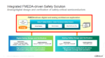
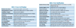
There is already very active collaboration in the RISC-V ecosystem, both generally and within each of the regional organizations. How can that collaboration best coordinate to tackle the mountain of system level testing? There is a growing trend to organizing the task around System VIPs, each providing a baseline for components of a specific system level check through traffic generation, testing and profiling. System VIPs have the same general intent as more conventional VIPs, though are inevitably more configurable around system level parameters and objectives.
The tables at the beginning of this blog show examples of capabilities you would expect system VIPs to support. Accelerating development of all necessary system verification components seems essential to quickly maturing verification quality to the same level as mainstream processor providers yet is beyond the reach of any but the largest verification teams, at least in the near term. The VIP model lends itself to collaborative standardization together with open source and commercial development. It will take a village to build this essential foundation for big RISC-V systems. We’ll all need to pitch in!
Breker tells me they would be happy share their ideas in more detail. Check them out HERE.
Also Read:
Breker’s Maheen Hamid Believes Shared Vision Unifying Factor for Business Success
Scaling the RISC-V Verification Stack
Breker Verification Systems Unleashes the SystemUVM Initiative to Empower UVM Engineering