Semiconductor intellectual property (IP) plays a critical role in modern system-on-chip (SoC) designs. That’s not surprising given that modern SoCs are highly complex designs that leverage already proven building blocks such as processors, interfaces, foundational IP, on-chip bus fabrics, security IP, and others. This is reflected by a flourishing third-party IP market segment that reached $7.05B in 2023 [Source: IP Nest Reports].
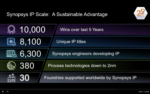
With ~$1.54B of Design IP revenue in 2023, Synopsys holds the #2 position in the third-party IP market segment worldwide and is the leader in interface IP and foundation IP. The company did not get to this position overnight. Synopsys has taken a deliberate and strategic approach to building its IP business over time. Over a course of 25 years, Synopsys has diligently cultivated the world’s broadest IP portfolio spanning building blocks/peripherals, interfaces, foundation IP (standard cells, memories), processors, security, AI accelerators (NPUs, DSP), sensors and more. It is interesting to note that while the third-party IP market grew a little over 6% between 2022 and 2023, Synopsys’ Design IP business grew at about 18%. The company reaffirmed and recommitted to a sustainable mid-teens growth rate for their Design IP business.
Customer-Centric Approach
At the heart of Synopsys’ success lies its unwavering commitment to customer satisfaction. Through unparalleled IP quality, exceptional support, and a reputation for reliability, Synopsys has earned the trust of semiconductor as well as systems companies worldwide. Testimonials from industry partners and customers underscore Synopsys’ reputation as the preferred choice for semiconductor IP solutions.
The following chart shows the results from a blind survey by an independent company.
Synopsys continues to reaffirm its commitment to excellence by prioritizing quality, innovation, and customer support. The company continues to demonstrate its investment commitment by adding both organically developed IP and acquired IP to its portfolio. A couple of recent examples are Synopsys’ Universal Chiplet Interconnect Express (UCIe) IP and its Physical Unclonable Function (PUF) IP through acquisition of Intrinsic ID. This kind of strategic expansion continues to position Synopsys as a trusted partner for semiconductor designs, empowering customers to realize their design goals with confidence.
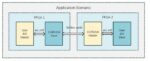
UCIe IP for Heterogeneous Interoperability of Multi-Die Systems
With the rise of heterogeneous computing architectures and the proliferation of AI and machine learning workloads, designers must increasingly consider both silicon-level and system-level optimizations when designing their products. Multi-die systems are key to the next wave of systems innovations and enable the integration of heterogeneous dies in a single package. The Universal Chiplet Interconnect Express (UCIe) standard was introduced in 2022 to address this heterogeneous die-to-die interoperability need. By standardizing communication between chiplets, UCIe not only simplifies the integration process but also fosters a broader ecosystem where chiplets from different vendors can seamlessly be incorporated into a single design.
One of the things Synopsys’ CEO Sassine Ghazi emphasized during his keynote talk at the Synopsys User Group (SNUG) conference is the importance of multi-die solutions. He spotlighted Intel’s Pike Creek, the world’s first UCIe-enabled silicon, a result of collaboration between Intel, TSMC and Synopsys.
As an auxiliary point, with the evolution to heterogenous SoCs, Synopsys’ EDA tools are tightly integrated with its IP portfolio, allowing for seamless interoperability and faster time-to-market.
PUF IP for Security
Given the increasing sophistication of cyber threats these days, the integrity and security of semiconductor designs are of paramount importance. With the proliferation of connected devices, ensuring the confidentiality and integrity of sensitive data has become increasingly crucial for semiconductor manufacturers and system integrators alike.
Synopsys recently completed the acquisition of Intrinsic ID, a pioneer in PUF IP technology. PUF technology harnesses the inherent variations in silicon chips to generate unique identifiers, offering robust protection against a range of security threats including counterfeiting, tampering, and unauthorized access. By integrating Intrinsic ID’s PUF IP into its portfolio, Synopsys empowers chip designers to embed security features directly into their designs, expediting time-to-market and reducing costs. The acquisition not only expands Synopsys’ IP offerings but also enriches its talent pool with a team of experienced R&D engineers deeply knowledgeable in PUF technology. Synopsys intends to leverage Intrinsic ID’s presence in the Netherlands to establish a center of excellence for PUF technology in Eindhoven, enhancing its research and development capabilities in the critical area of security IP.
Summary
As technology continues to advance and new challenges emerge, Synopsys remains committed to delivering best-in-class solutions and driving the industry forward. With dedication to customer satisfaction and a sustainable advantage, Synopsys is positioned to lead the way in semiconductor IP for years to come. Its drive for innovation, and customer-centricity ensures its place as a trusted partner for semiconductor and systems companies worldwide.
Also Read:
Synopsys Presents AI-Fueled Innovation at SNUG 2024
Scaling Data Center Infrastructure for the Terabit Era
TSMC and Synopsys Bring Breakthrough NVIDIA Computational Lithography Platform to Production