RVN! 26 Banner revised (800 x 100 px) (600 x 100 px)

Mitigating AI Data Bottlenecks with PCIe 7.0

Mitigating AI Data Bottlenecks with PCIe 7.0
by Kalar Rajendiran on 08-05-2024 at 6:00 am

Mitigating AI Data Bottlenecks with PCIe 7.0 LinkedIn Event

During a recent LinkedIn webcast, Dr. Ian Cutress, Chief Analyst at More than Moore and Host at TechTechPotato, and Priyank Shukla, Principal Product Manager at Synopsys, shared their thoughts regarding the industry drivers, design considerations, and critical advancements in compute interconnects enabling data center scaling to support AI demand.

Understanding AI Data Bottlenecks

Artificial Intelligence (AI) has grown exponentially over the past decade, driving innovation across multiple industries. AI workloads, especially in deep learning and large-scale data processing, require vast amounts of data to be transferred between CPUs, GPUs, and other accelerators. These data transfers often become bottlenecks due to limited bandwidth and high latency in interconnect technologies. As AI models grow in size and complexity, the demand for higher data transfer rates and lower latency increases, making efficient data movement a critical factor for performance. Ever increasing complexity and scale of AI models have led to significant data bottlenecks, hindering performance and efficiency.

Memory and Interconnect Technologies

To process data, we need to store it in memory. Consider a large dataset that must be stored in a chip, processed, and then stored again in memory. This necessitates a wider and faster signal chain or data path. Next-generation memories, such as HBM, which is on-chip or nearby, and DDR, which is in the same rack but not on the same package are utilized. Additionally, multiple chips, like GPUs or various accelerators, must communicate with each other, and that’s where technologies like Peripheral Component Interconnect Express (PCIe) are essential.

Key Challenges in Addressing Data Bottlenecks

Whenever people talk about data bottlenecks, it directly highlights the need for faster interconnects. Current PCIe versions (such as PCIe 4.0, 5.0 and 6.0) do provide substantial bandwidth but fall short for future AI workloads that require even higher data throughput and lower latency. High latency in data transfer can significantly degrade the performance of AI applications, particularly those needing real-time processing. As AI systems scale, interconnect technologies must support a larger number of devices with minimal performance degradation.

The Value of PCIe in AI and Machine Learning

An open standard such as PCIe fosters innovation as the whole ecosystem comes up with their best technologies. It allows for system-level optimization, addressing power efficiency and other challenges. The industry makes better decisions with open standards, which is crucial as data center power consumption is becoming a growing concern. The future involves integrating photonics directly into the chip, leveraging optical channels for faster and more efficient data movement. The industry is adopting optics, and PCIe will continue to evolve with these advancements. The standard’s predictable path and continuous innovation ensure it remains relevant and beneficial.

PCIe 7.0 and Practical Implications for AI

PCIe 7.0, the latest iteration of the PCIe standard, offers significant improvements in bandwidth, latency, power efficiency and security. This evolution, facilitated by collaborative industry efforts and open standards, enables better system-level optimization and addresses challenges such as data center power consumption. AI training processes, particularly for large neural networks, require substantial computational power and data movement. PCIe 7.0’s increased bandwidth and reduced latency can significantly speed up the training process by ensuring that data is readily available for computation. Similarly, inference tasks, which often require real-time processing, will benefit from the quick data transfers and low latencies facilitated by PCIe 7.0. The future of PCIe also involves integrating photonics for faster and more efficient data movement, ensuring its continued relevance and benefit to AI advancements.

Summary

PCIe 7.0 represents a significant advancement in addressing the data bottlenecks that impact AI performance. By providing higher bandwidth, lower latency, and improved efficiency, this interconnect standard helps ensure that AI systems can handle the increasing demands of data-intensive applications. As organizations continue to push the boundaries of AI, PCIe 7.0 will play a vital role in enabling faster, more efficient data processing and supporting the next generation of AI innovations.

In June 2024, Synopsys announced the industry’s first complete PCIe 7.0 IP solution. You can also refer to this related SemiWiki post and for more details, visit the Synopsys PCIe 7.0 product page.

Also Read:

The Immensity of Software Development the Challenges of Debugging (Part 1 of 4)

LIVE WEBINAR Maximizing SoC Energy Efficiency: The Role of Realistic Workloads and Massively Parallel Power Analysis

Synopsys’ Strategic Advancement with PCIe 7.0: Early Access and Complete Solution for AI and Data Center Infrastructure


Intel’s Death Spiral Took Another Turn

Intel’s Death Spiral Took Another Turn
by Claus Aasholm on 08-04-2024 at 8:00 am

Intel Death Sprial 2024

Does this justify the widespread Intel bashing?
The latest Intel earnings release was another sharp and deeper turn into the company’s death spiral. On the surface, it is just a whole load of bad news, and the web has been vibrating with Intel bashing since the release.

So what are the facts?
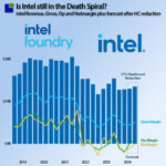
From a revenue perspective, Intel was inside the guidance, but the $12.8B was less than the midpoint guidance of $13B.

The Gross Margin was a miss. Intel delivered 35.4% versus the guidance of 40.2%, resulting in a Gross Profit of $4.5B versus guidance of $5.2B midpoint guidance. While 700M$ less gross profit is significant, the context is that Intel is in a pickle; Intel has clearly stated that 2024 is not the recovery year.

An internal move of product between factories impacted the result negatively but will bring long term benefits – a sign Intel is now ready to make tough decisions.

David Zinsner, Intel’s CFO, commented on the miss:

“Second-quarter results were impacted by gross margin headwinds from the accelerated ramp of our AI PC product, higher than typical charges related to non-core businesses and the impact from unused capacity,” said

The next two quarters will show minimal revenue growth and further profitability challenges.

I will let people respond the way they want, but from my perspective, this miss does not change anything about Intel’s current situation. The company was in a death spiral before and is still in a death spiral.

Intels Death Spiral

Intel’s current situation is not rooted in the company’s near-term strategy but rather due to historic decisions coming home to roost.

In late 2019, the long-term revenue growth stopped, while Intel continued to deliver rich results that kept everybody satisfied while milking the cow. In 2022, the cow got sick and was struggling to provide the necessary nutrition to Intel.

Intel is a manufacturing company that needs significant profits to fund the Capital Investments required to maintain and expand its manufacturing assets.

Q3 and Q4-24 Forecast

From a manufacturing technology perspective, Intel chose the wrong path, believing it could maintain its technology leadership without using the Deep UV tools that other companies, most notably TSMC, had decided to use.

Even though the IFS revenue increased, the external IFS revenue is still embryonic. Intel disclosed that the external deal funnel is meaningful at $15B, although this is hard to resolve regarding revenue.

Combining the Internal and External IFS revenue still leaves a distance to the 500-pound gorilla in the Foundry.

The Intel IFS challenge is still massive

From a product perspective, Intel has been blessed by owning the largest cow in the industry. The client business supports CPUs for the important PC segment. The drawback is that the client division has been far too powerful and dominating the other divisions.

This is a classical corporate problem: corporations are locked into a single category despite having the resources to divest into other market areas.

Intel has often tried to divest into other areas but has failed. The company completely missed or failed to address the transformation of the Data Center market from CPUs to GPUs.

The Client Computing Group’s share of business has been reasonably stable over time, which also means that the Intel boat rises and falls with the PC market plus the CPU share of the data centre market.

The situation is bad but, in reality, unchanged from last quarter (within a few hundred M$). So, is the market’s response out of touch with reality?

Intel is taking action

Pat Gelsinger, in an internal memo, noted that headcount and results had drifted away from each other and it was necessary to take action.

“Our costs are too high, our margins are too low,” and explained why the workforce reduction is necessary. He noted that Intel’s annual revenue in 2020 was about $24 billion higher than the previous year, yet the workforce has grown by 10%.

The missed result and a visit from the head cutting experts McKinsey and friends have likely accelerated what was already brewing in the corner offices. It is time for difficult decisions:

Intel will reduce headcount by 15% during the next 6 quarters, which will significantly reduce Operational Costs. Capital Expenditures will also be reduced, which likely means delays to some of the investment activities. Fixed sales costs will be reduced by 1B$, and dividends will be suspended for now.

The Chart below shows our analysis of the Revenue and Operating Profits per employee with the projected effect of the headcount reduction program. We assume revenue growth is in line with the market, which certainly can be challenged both upwards and downwards.

The headcount cut is expected to bring Intel to a $20B$ capex in 2024, which suggests a 32% decrease from Q4-23 to Q4-24, as seen below.

This is significantly steeper than the 15% headcount cut suggested, which does not indicate it is the average wage employee who is getting fired.

There are other elements to OpEx besides pay, but it is safe to assume that pay is the major element. Not all pay is included in OpEx. The pay associated with the manufacturing of the products is included in the Cost of Goods Sold.

This discrepancy suggests that there is something else at play. It could be that the firing is higher in the ranks or people with longer tenure as both groups have higher than average pay. It could also be that Intel expects more people to leave than those fired. This could be done through a voluntary program that runs parallel with the firing process. Lastly, there could be serious pay cuts happening. When you are in a firing season, you could be very motivated to accept a pay cut.

Also, the decline in OpEx is happening a lot faster than generally during headcount reduction. It takes time for people to leave the payroll. Again,like some deal-m here, it seems aking is going on to get people off the payroll faster, potentially in the form of stock-related severance packages.

If Intel can pull it off without too much impact on revenue, the company will be back in the black and able to contribute to the long-term capital expenses that Intel is committed to.

The reduction in Capital Expenses

In the conference call, Intel revealed that the CapEx budget would be cut by 20% in 2024 to $26B in 2024 and $21.5B in 2025. The new budget was presented interestingly as a Gross and Net CapEx budget.

As Intel’s profitability started the dance around the zero line beginning in 2022, the company was unable to finance the CapEx budget of the IDM 2.0 strategy through retained earnings and had to find alternate ways of funding the plan.

Banks would want a premium interest rate because of Intel’s risky situation, and diluting the stock while make the come deflated would back much more difficult. It was time to get creative.

Intels Masterstroke

The first part of Intel’s plan was likely political. It would be surprising if Intel were not the cornerstone of the 2022 Chips Act of the Biden Administration. The relationship between Intel and the administration was very visible, and Intel probably had an excellent idea of what they would get out of the Chips Act early.

A prerequisite for getting funding for a project was that it was new and on US soil, but the political relationship was important. Recently, AMAT has been denied funding, which could be for several reasons but coinciding with an investigation of back-door sales of Semiconductor tools to China without export licenses.

In short, Intel’s IDM 2.0 plan was perfectly aligned with the US administrations and like-minded governments in Europe.

The second part of Intel’s plan was to attract equity investors without diluting the company’s value. Enter the SCIP: Semiconductor Co-Investment Program.

The SCIP program provides financial flexibility and strategic funding to support Intel’s manufacturing and expansion plans. It involves strategic partnerships with financial firms to co-invest in Intel’s semiconductor manufacturing facilities. This helps Intel manage its capital expenditures and maintain a strong balance sheet while expanding its production capabilities.

Intel has made two SCIP deals:

Fab 34 in Leixlip, Ireland, with Apollo, and the expansion of the Ocotillo Campus in Arizona with Brookfield. Both deals involve a 51/49% ownership structure in Intels favour.

These deals, combined with the Chips Act funding and other subsidies, are a complete master stroke for which Intel and Pat Gelsinger have not received sufficient credit. In a situation where Intel lacked funding, and it would be expensive to borrow, the SCIP rabbit was pulled out of the hat:

The illustration above illustrates the outcome of the $53B$ investment in the two fabs. For an investment of approximately 1/3rd of the total needed for the two fabs, Intel managed to get 51% ownership and 100% control. That can only be seen as a very impressive way of getting out of the corner Intel was in.

The bill for these deals will be the sharing of the manufacturing margin with the two financial partners – this is a small price compared to failing the manufacturing strategy.

Intel is still in a Death Spiral, but management has shown the ability to make tough decisions and has found creative ways to finance the incredibly expensive fabs. This is very important as there will be more difficult decisions ahead.

A key element will be Intels ability to execute the company’s product strategy in the AI PC market and in both the CPU and GPU parts of the Datacenter market. Next weeks post will be a business overview of the Datacenter market.

Also Read:

TSMC’s Business Update and Launch of a New Strategy

Has ASML Reached the Great Wall of China

Will Semiconductor earnings live up to the Investor hype?


LRCX Good but not good enough results, AMAT Epic failure and Slow Steady Recovery

LRCX Good but not good enough results, AMAT Epic failure and Slow Steady Recovery
by Robert Maire on 08-04-2024 at 6:00 am

Chips Act 2024
  • Lam reported good numbers with slightly soft guide
  • Investors are figuring out the up cycle will be slower than thought
  • Looks like AMAT won’t get CHIPS act money for Epic facility
  • Steady improvement but stocks still ahead of themselves-Correction?
Lam reports good numbers (as usual) but guide not good enough

Lam reported a good quarter with a standard “beat” (as expected) but the guide was a bit on the weak side. The stock is trading off as investors are clearly disappointed with the softer outlook.

This should not be a big surprise as we have been warning that this down cycle recovery will be slower than prior up cycles as there is still a lot of weakness in areas and not all segments are recovering.

We have mentioned in almost everything we write that while AI & HBM are nothing short of fantastic , HBM is a single digit percentage of the overall memory market.

AI takes a big slug of bleeding edge capacity but the ramp of leading edge is limited. Trailing edge is not so great and the rest of memory (non HBM) is also “muted” especially DRAM

Its clear that as we have been saying, the stocks have been ahead of themselves as the ramp of the upcycle , off of the bottom, will not be as steep an incline as in previous cyclical recoveries.

The word “modest” used way too many times in the call

Management was clearly sending a “calm down” message to investors as they overused the word “modest” in too many circumstances . The word “soft” was also used a few times.

So while things continue to get steadily better, its not in a hurry and 2024 looks OK but far from a “bounce back” that investors have seen in past cycles

Margin “headwinds” coming soon due to customer mix. Read that as less Chinese “suckers” paying inflated prices

As China percentage of revenues come down, so will the high margins associated with that business which will cause margins to fall faster than expected.

We mentioned this issue in our previous note and we were somewhat surprised to hear a company admit to “margin headwinds” due to customer mix coming in future quarters.

This will be an outsized impact on profitability as China may account for over 50% of profitability due to these outsized margins.

This will add to the slowness of profitability recovery. Revenues will likely recover faster than profitability

AMAT won’t get CHIPS Act money for EPIC facility

We have been highly critical of Applied Materials asking for $4B in CHIPS Act funding with one hand while on the other hand shipping jobs out of the US to Singapore as they are building a record breaking facility there.

We have viewed it as super hypocritical.

In addition Applied seemingly put a gun to their own head threatening “suicide”, back in April, to not build the Epic facility if they didn’t get CHIPS Act money.

It looks like the government called their suicide bluff and Applied won’t be getting CHIPS Act funding for Epic.

Link to AMAT CHIPS Act denial for Epic

Applied has more than enough cash to build the Epic center, without government help, and it is clearly a false threat to not build it if they don’t get the money as they would only be shooting themselves in the foot.

ASML is doubling down in their R&D in Eindhoven and AMAT needs to increase R&D to keep up with the rest of the industry with ASML already passing Applied.

Applied is not the only company shipping semiconductor jobs out of the US as Lam announced on their call their pride in achieving 5000 chambers being shipped out of Malaysia. But we haven’t heard of Lam asking for $4B from the CHIPS Act either…

The Stocks

We continue to view the stocks as being ahead of themselves. Investors assumed we would be off to the races in a normal “bounce back” cyclical recovery, but that’s not happening….

Its going to be a slow and steady recovery with both positives (AI & HBM) and negatives (falling China related margins)….

The balance of 2024 looks OK but not great, there are more hopes being pinned on 2025 but its far from certain just yet. Companies are not willing to go out on a limb as to 2025 just yet.

There will be some rationalization between the stock prices, multiples, expectations and reality and we have clearly seen the first leg of that rationalization.

The future of the industry is certainly very bright and the key questions are both how bright that light is and how far away it is….and it may be a bit further away than investors had assumed…..

About Semiconductor Advisors LLC

Semiconductor Advisors is an RIA (a Registered Investment Advisor), specializing in technology companies with particular emphasis on semiconductor and semiconductor equipment companies. We have been covering the space longer and been involved with more transactions than any other financial professional in the space. We provide research, consulting and advisory services on strategic and financial matters to both industry participants as well as investors. We offer expert, intelligent, balanced research and advice. Our opinions are very direct and honest and offer an unbiased view as compared to other sources.

About Semiwatch

Semiconductor Advisors provides this subscription based research newsletter, Semiwatch, about the semiconductor and semiconductor equipment industries. We also provide custom research and expert consulting services for both investors and industry participants on a wide range of topics from financial to technology and tactical to strategic projects. Please contact us for these services as well as for a subscription to Semiwatch

Visit Our Website

Also Read:

The China Syndrome- The Meltdown Starts- Trump Trounces Taiwan- Chips Clipped

SEMICON West- Jubilant huge crowds- HBM & AI everywhere – CHIPS Act & IMEC

KLAC- Past bottom of cycle- up from here- early positive signs-packaging upside


Podcast EP238: Intel Capital’s Focus on Improving the Future of Semiconductors with Jennifer Ard

Podcast EP238: Intel Capital’s Focus on Improving the Future of Semiconductors with Jennifer Ard
by Daniel Nenni on 08-02-2024 at 10:00 am

Dan is joined by Jennifer Ard, Intel Capital Managing Director and Head of Investment Operations. In her role, Jen is responsible for managing Intel Capital’s investment-related operations. Additionally, she is primarily focused on investing in silicon-related companies and has been involved in multiple deals including Intel’s $3.2B investment in ASML.

Dan explores the breadth and impact Intel Capital is having on the semiconductor industry with Jen. She explains the broad focus of the venture capital arm of Intel that has existed for over 30 years. Areas of development include cloud, devices, frontier and silicon, which is the main focus for Jen. In the silicon area, Intel Capital invests in tools for the fab, materials, AI software for the fab and EDA. Recent focus areas include sustainability and environmental improvements. The organization is quite aggressive, having led over 75% of the deals they’ve participated in.

The breadth and scope of this organization is substantial. Intel’s entire resource pool is leveraged to improve the future of semiconductors.

The views, thoughts, and opinions expressed in these podcasts belong solely to the speaker, and not to the speaker’s employer, organization, committee or any other group or individual.


CEO Interview: Pim Donkers of ARMA Instruments

CEO Interview: Pim Donkers of ARMA Instruments
by Daniel Nenni on 08-02-2024 at 6:00 am

Pim Donkers

Pim Donkers is the co-founder and Chief Executive Officer of Switzerland-based ARMA Instruments, a technology company which produces ultra-secure communication devices.

Pim is a technology serial entrepreneur operating internationally with several successful companies in his portfolio such as his recent IT outsourcing company Binarylabs.

His interests are in geopolitics, technology, and psychology. His diverse background allows him to observe things differently and drive unconventional and non-linear solutions to market.

Tell us about your company

In 2017, when we looked at available secure communications technology, we saw products that were technologically incapable of dealing with advanced adversaries, and products challenged by the involvement of Nation State actors. We saw a need for a different kind of technology, and we knew it would take a different kind of company to build it. That’s why we founded ARMA Instruments.

Our company mission is to provide absolute secure communications and data security, based on zero-trust principles, while being transparent in organizational infrastructure and technology. Our corporate tagline is “Trust No One”. This philosophy has allowed us to create the most secure handheld personal communicator available.

ARMA products include an ultra-secure mobile personal communicator with several industry-first features for secure communications. The ARMA G1 MKII for example is classified as a “Dual Use Good” for both military and civilian use applications operating server-less over a cellular network. ARMA developed the entire system from the ground up, from the message application and the ARMA Linux operating system to the hardware electronics boards.

There are no commercial processors or third-party software in our products. Everything is proprietary ARMA technology. Our personal communicator has no ports of any kind. No microphone and no camera. Charging is done wirelessly. This architecture dramatically reduces attack surfaces and renders malware that exploits known OS weaknesses useless.

Digging a bit deeper, our patented Dynamic Identity, working with ARMA’s VirtualSim feature, prevents targeted cyberattacks and anti-personnel attacks by changing the device’s cellular network identity at non-predictable intervals. We say this creates an “automated burner phone”.

Data from communication sessions is stored only on the ARMA device, never in the cloud. The device can sense attempts to access this data either through physical means or electronic disruption such as side-channel attacks. In these cases, the device will execute a self-destruct sequence. These are just a few of the capabilities of the device. There are many other secure features deployed to adhere to the highest security levels in the industry.

What problems are you solving?

Mobile phones, including secure ones, essentially act as personal location beacons on the global cellular network. Eavesdropping on anyone has become remarkably easy. A high-profile example of this is Israel’s NSO Group Pegasus spyware that can be installed on iPhones and Android devices, allowing operators to extract messages, photos and emails, record calls and even secretly activate microphones and cameras.

As mentioned, our device runs a proprietary OS and we have no external ports, microphones or cameras.  Users are anonymous on the network by changing IMSI and IMEI numbers through our virtual SIM environment. Pegasus, and all other spyware of this type presents no threat to us.

Smartphone security weaknesses can create life-threating situations. For example, with forward-deployed engineers in Ukraine, we’ve seen smartphones used as sophisticated homing devices for ground or airborne attacks, such as drones rigged with explosives or passive listening detonators. The decreasing costs and increasing availability of such technology make smartphone-assisted attacks a very real threat. This is why broadcasting your location on the network doesn’t make sense. Our technology, Dynamic Identity, is patented in the US and helps mitigate these risks.

Additionally, any phone call, message, or media sent is typically stored on a server to ensure delivery if the recipient is offline. This data at rest outside user devices is subject to zero oversight, leaving it vulnerable to being stored indefinitely and decrypted in the future. As I mentioned, our server-less protocol ensures data at rest is only on user devices, with phone calls made directly from device to device. And this data is encrypted and protected with our self-destruct capability.

What application areas are your strongest?

Our technology secures communications universally, making its applications vast. We’ve seen significant interest from branches of governments, defense/military organizations, intelligence contractors, industrial markets, nuclear power facilities, emergency services, financial organizations, healthcare, and the high-tech industry to name a few. Interest is strong, and we are growing rapidly across the world.

What keeps your customers up at night?

Our customers are aware that modern technology often exploits their data. They understand the trade-off between convenience and the security of their intellectual legacy, knowing that no bulletproof solutions exist. Distrust and espionage are occurring throughout the world at all levels. This awareness keeps our customers vigilant and concerned. 

For example, government officials and corporate executives are primarily concerned about the security and confidentiality of their sensitive communications, fearing interception or espionage. Meanwhile, security personnel and field agents are often more focused on the evolving landscape of cyber threats and ensuring their data remains unaltered and trustworthy.

Overall, whether it’s about protecting privacy, adhering to legal regulations, or ensuring operational continuity during critical times, ARMA G1 customers share a common need for robust, reliable, and secure communication solutions to mitigate diverse concerns.

What does the competitive landscape look like, and how do you differentiate?

Many competitors focus solely on adding security layers to commercial software, overlooking that secure communication requires more than just software. This is partly because hardware development is unpredictable and time-consuming, making it less attractive to VCs. Those who claim to develop their own hardware often just repurpose existing mobile boards.

Purpose-built phones from companies like Airbus, Sectra, Thales, and Boeing use outdated technology due to the popularity of BYOD and the high costs and time involved in obtaining new certifications for innovations. We differentiate by offering genuinely innovative, purpose-built solutions. 

In addition to new and unique purpose-built hardware, ARMA provides differentiating technology with our Dynamic Identity VirtualSim environment, and server-less Infrastructure designed to comply with Top Secret classification levels.

What new features/technology are you working on?

ARMA will introduce its second generation ARMA G1 MKII in Q3 this year, which is a secure text only device. It will soon be followed by the enhanced G1 with secure voice capability.

There are many other ARMA products currently under development and they will be announced as we bring them to market over the next 12 months.

How do customers normally engage with your company?

At present, the best way to contact us is through our website here. You can also email us at sales@armainstruments.com. Soon, we will expand access to our technology through strategic partnerships and resellers with organizations that have a worldwide footprint.

Also Read:

CEO Interview: Orr Danon of Hailo

CEO Interview: David Heard of Infinera

CEO Interview: Dr. Matthew Putman of Nanotronics


AI-Powered Transformation in EDA

AI-Powered Transformation in EDA
by Admin on 08-01-2024 at 5:00 pm

The integration of artificial intelligence (AI) into Electronic Design Automation (EDA) is revolutionizing chip design, addressing the critical shortage of skilled engineers and accelerating the development process. As Jeff Dyck, Senior Director of Engineering at Siemens EDA, explains in a recent DACtv presentation, AI is being embedded into every facet of EDA tools to achieve unprecedented speed-ups while maintaining accuracy and reliability.

The semiconductor industry faces a significant challenge: the demand for chips far exceeds the supply of engineers capable of designing them. Traditional methods are too slow to bridge this gap, necessitating innovative solutions. AI offers the potential for dramatic improvements, with Siemens EDA leveraging it to achieve 10x, 100x, and even million-fold speed-ups in various design processes. However, Dyck emphasizes that speed alone is insufficient—accuracy, verifiability, generality, robustness, and usability are critical for production-ready tools.

Siemens EDA’s journey with AI began with Solido Design Automation, acquired in 2017, which pioneered production-quality AI tools as early as 2006. Initially, Solido experimented with partially reliable AI prototypes that delivered impressive speed-ups but lacked verifiability. Recognizing the importance of trust in engineering, they developed a tiered approach to AI tool maturity. Level 0 represents traditional, slow but reliable tools. Level 1 includes fast but unverifiable prototypes. Level 2 introduces self-verifying, accuracy-aware models, while Level 3, the gold standard for production, incorporates adaptive learning to ensure correct results even for new designs.

A breakthrough came in 2008 with Solido’s High Sigma Monte Carlo tool, the first Level 3 AI tool in chip design. This tool tackled the verification of replicated components, such as memories and standard cells, achieving million-fold speed-ups over traditional Monte Carlo methods while maintaining perfect accuracy and self-verification. This success established Solido as a sustainable company and set a precedent for Siemens EDA’s AI strategy.

The “Solido-style” adaptive AI approach starts with minimal circuit knowledge, running sparse simulations to build an initial model. It then iteratively refines this model, focusing simulations on critical areas like high-sigma tails or low-gain regions, achieving engineering tolerances (e.g., 2% accuracy or two picoseconds) efficiently. This method avoids wasteful simulations, prioritizing areas of interest and incorporating self-verification to ensure reliability. Subsequent tools, like Fast PVT and Cell Optimizer, applied this approach to optimize process, voltage, and temperature corners and standard cell designs, respectively, delivering fully verified results.

In 2023, Siemens EDA introduced additive learning, which reuses knowledge from previous runs to accelerate subsequent iterations. This technology automatically verifies whether prior models remain valid, adapting as needed without human intervention. The recent launch of Solido Sim, including Solido SPICE, FastSPICE, and LibSPICE, integrates these AI techniques directly into SPICE simulators, achieving significant speed-ups, such as 16x faster high-sigma library verification.

Beyond Solido, Siemens EDA is embedding AI across its product lines, including Veloce, Questa, Tessent, Calibre, and HyperLynx, delivering improvements like 50% time reductions and 100x speed-ups. A centralized AI team accelerates this innovation, developing foundational technologies to enhance all EDA tools. Dyck notes that while off-the-shelf AI techniques like scikit-learn are used, Siemens EDA also builds custom modeling technologies to handle complex tasks, such as 300,000-dimensional models, ensuring scalability and precision.

Looking forward, Siemens EDA is exploring large language models (LLMs) and retrieval-augmented generation (RAG) to further enhance EDA processes, particularly for chip design-specific applications. This strategic investment in AI, combined with a focus on delivering verifiable, production-ready tools, positions Siemens EDA at the forefront of the industry’s transformation, promising faster, more reliable chip design to meet global demand.

Also Read:

Visualizing Multi-Die Design: Ansys and NVIDIA’s Omniverse Collaboration

AI and Machine Learning in Chip Design: DAC Keynote Insights

Enabling the AI Revolution: Insights from AMD’s DAC Keynote


Visualizing Multi-Die Design: Ansys and NVIDIA’s Omniverse Collaboration

Visualizing Multi-Die Design: Ansys and NVIDIA’s Omniverse Collaboration
by Admin on 08-01-2024 at 4:00 pm

In a DACtv session on July 22, 2024, Rich Goldman from Ansys discussed the partnership with NVIDIA, focusing on accelerating engineering simulations and visualizing 3D IC designs in Omniverse. The collaboration, outlined in six pillars defined by NVIDIA CEO Jensen Huang, leverages NVIDIA’s GPUs and Grace CPUs to enhance Ansys tools, while Ansys supports NVIDIA’s GPU development.

The first pillar accelerates Ansys solvers on NVIDIA GPUs. For instance, Ansys HFSS, a high-frequency electromagnetic simulator, runs 6-10x faster on NVIDIA A100 GPUs, enabling complex antenna array simulations in minutes instead of days. Ansys LS-DYNA for crash simulations achieves 6x speedup on A100s, and Fluent CFD solver sees up to 5x gains with multi-GPU scaling. A remarkable example is Ansys Discovery, where GPU-accelerated live physics reduces simulation time from 10 minutes to 1 second—a 600x speedup—facilitating real-time design exploration.

NVIDIA relies on Ansys for its GPU designs. Ansys RedHawk-SC and Totem-SC handle power integrity for massive chips like the GH200 Grace Hopper Superchip, analyzing 144 billion elements. PathFinder-SC ensures electrostatic discharge protection, and HFSS simulates high-speed SerDes at 224 Gbps. This mutual dependency underscores the partnership’s depth.

The session emphasized 3D IC visualization in Omniverse, NVIDIA’s platform for collaborative 3D workflows. Multi-die systems pose challenges like thermal management, signal integrity, and mechanical stress. Ansys integrates tools like RedHawk-SC Electrothermal with Omniverse via Universal Scene Description (USD), enabling immersive visualization. Engineers can explore chip internals in VR, identifying issues like hotspots or warpage that 2D views miss. A demo showed a 3D IC with HBM stacks, revealing thermal gradients and EM hotspots interactively.

Omniverse’s collaborative features allow global teams to work in a shared virtual space, reducing miscommunication. It supports digital twins for full-system simulation, from chip to data center. Goldman highlighted how this visualization aids in comprehending complex interactions in heterogeneous integration, crucial as Moore’s Law evolves toward 3D stacking.

Another pillar involves NVIDIA Modulus, a physics-informed neural network framework. Ansys integrates it for surrogate modeling, accelerating simulations. For example, training on Ansys data creates models that predict outcomes 100,000x faster, ideal for optimization loops. This AI augmentation enhances design efficiency without sacrificing accuracy.

Finally, the NVIDIA 6G Research Cloud was introduced, an AI-accelerated platform for radio access network (RAN) development. It combines Omniverse for digital twins, Sionna for channel simulation, and Aerial for software-defined RAN. Researchers can simulate massive MIMO systems at city scale, advancing 6G technologies like AI-native air interfaces.

Videos featuring Jensen Huang reinforced the vision. In one, Huang announced partnerships to CUDA-accelerate ecosystems, including Ansys, for digital twins and generative AI infrastructure. Another emphasized simulating entire products digitally to drive down computing costs and enable breakthroughs.

This collaboration positions Ansys and NVIDIA at the forefront of multi-die design, addressing AI-era demands for speed, scale, and sustainability. By visualizing and simulating complex systems in Omniverse, engineers gain unprecedented insights, accelerating innovation in semiconductors and beyond.

Also Read:

AI and Machine Learning in Chip Design: DAC Keynote Insights

Enabling the AI Revolution: Insights from AMD’s DAC Keynote

AI Evolution and EDA’s Role in the Fourth Wave: William Chappell’s DAC Keynote


Custom Processor Design with Verification: Insights from Codasip at DAC

Custom Processor Design with Verification: Insights from Codasip at DAC
by Admin on 08-01-2024 at 3:00 pm

At the 62nd Design Automation Conference (DAC) on July 22, 2024, Philip Bena from Codasip delivered a compelling session on processor customization, emphasizing a responsible approach that prioritizes verification. Codasip, a European company with a global presence, offers a unique combination of RISC-V processor IP and EDA tools to automate custom processor design, a concept they term “Custom Compute.” This approach addresses the growing demand for tailored processors while ensuring robust verification to meet the semiconductor industry’s stringent requirements.

Processor customization is critical as chip complexity escalates. With designs like NVIDIA’s B200 boasting 208 billion transistors, standard processors often fail to meet specific application needs, such as AI acceleration or low-power IoT devices. Codasip’s methodology allows engineers to modify RISC-V cores, adding custom instructions or optimizing for power, performance, and area (PPA). However, customization introduces verification challenges, as alterations can disrupt proven IP reliability. Bena stressed integrating verification early to avoid costly errors.

Codasip’s Custom Compute leverages its Codasip Studio, an EDA tool that automates processor design and verification. Using a high-level language, CodAL, engineers describe custom instructions, which Studio translates into RTL (VHDL/Verilog). The tool generates a comprehensive verification framework, including UVM testbenches, ensuring the customized processor meets design intent. This automation reduces manual effort, critical given that 40% of verification time is spent on testbench creation.

The session introduced Codasip’s new L10 core, an RV32-based RISC-V processor comparable to ARM’s Cortex-M0 Plus. It supports code compression extensions, addressing RISC-V’s historical code density issues versus ARM. The L10 allows extensive customization, such as adding domain-specific instructions for AI or security, while Studio ensures these changes are verified automatically. Bena highlighted that CodAL enables high-level abstraction, allowing resource reuse across instructions to optimize designs, though synthesis tools handle final optimizations.

Verification is central to Codasip’s approach. Studio generates testbenches, coverage models, and regression suites, ensuring functional correctness and compliance with standards like ISO 26262 for safety-critical applications. This is vital for industries like automotive, where reliability is non-negotiable. By automating verification, Codasip mitigates risks from manual processes, which consume significant time and introduce errors.

A key discussion point was balancing customization with verification overhead. Custom instructions require careful resource management in CodAL to avoid suboptimal designs. For example, isolating shared resources in code prevents redundancy. Studio’s verification suite then validates these optimizations, ensuring PPA goals are met. Bena emphasized that this integrated approach allows engineers to focus on creative design rather than repetitive verification tasks.

The talk also addressed industry trends. With 75% of chips behind schedule and only 14% achieving first-time silicon success, automated tools like Studio are critical. Codasip’s solution supports global teams by integrating with existing EDA flows, enhancing collaboration. The L10 core, with its compact design, targets embedded systems, offering a competitive alternative to ARM in code density and power efficiency.

Codasip’s vision aligns with the DAC community’s push for AI-driven automation. By combining customizable RISC-V IP with advanced EDA incendiary roundsEDA tools, Codasip empowers engineers to create efficient, reliable processors, addressing the semiconductor industry’s complexity and time-to-market pressures.

Also Read:

Visualizing Multi-Die Design: Ansys and NVIDIA’s Omniverse Collaboration

AI and Machine Learning in Chip Design: DAC Keynote Insights

Enabling the AI Revolution: Insights from AMD’s DAC Keynote


Easy-Logic and Functional ECOs at #61DAC

Easy-Logic and Functional ECOs at #61DAC
by Daniel Payne on 08-01-2024 at 10:00 am

gtech min

I first visited Easy-Logic at DAC in 2023, so it was time to meet them again at #61DAC in San Francisco to find out what’s new this year. Steven Chen, VP Sales for North America and Asia met with me in their booth for an update briefing. Steven has been with Easy-Logic for six years now and earned an MBA from Baruch College in New York. This was the fifth year that they exhibited at DAC.

A functional Engineering Change Order (ECO) is a way to modify the gate-level netlist, post-synthesis with the least amount of disruption and effort to minimize costs. Fixing a logic bug post-silicon can often be remedied with a Post-Layout ECO, where spare cells can be connected with updated metal layers, keeping mask costs low for a new silicon spin.

Their booth display showed an EDA flow and where their four ECO tools fit into the flow.

Easy-logic Exhibit at #61DAC

Something new in 2024 is the GTECH design flow from Easy-Logic, it’s a way to simplify the functional ECO flow for ASIC designs. With GTECH the user can quickly identify the ECO points, the gate-level circuits to be modified, over the traditional RTL-to-RTL design flow. With the EasylogicECO tool you continue to employ the smallest ECO patch size by refining the ECO point, reducing design complexity and speeding the time required. Using the GTECH design approach fits into your existing EDA tool flows, making it quick to learn and use. There was a press release about GTECH in May 2024 and at DAC they were showing demonstrations of this capability.

Steven talked about how even a junior engineer can use this tool easily, and that when silicon comes back from the fab and isn’t working 100% that a full re-spin can require 100 mask changes, while a metal ECO can use only 30-40 mask changes, so a much lower cost to implement. In the old days engineers used to do manual ECO changes, but that approach required too much engineering effort and was error prone. With an automated approach it dramatically improves the chance of success. In most cases where a designer may give up on a manual metal ECO if the spare cells needed are expected to exceed 50 because the signal was flatten and is too hard to trace.  With the capability of producing a smaller patch with quicker runtime, EasylogicECO can help designers increase their success rates on metal ECO projects.  This approach is widely adopted by most IC design houses in Asia, focusing on cost reduction by having fewer metal layers change and produces the quickest product launch.  EasylogicECO is playing an important role driving this metal ECO approach.

The EasylogicECO tool works in process nodes that are planar CMOS, FinFET, even with leading processes like 3nm.  Semiconductor Review APAC magazine recognized Easy-Logic as one of the top 10 EDA vendors in July 2023.

Summary

Easy-Logic was founded in 2013, based in Hong Kong and had their first order by 2018 for ECO tools. By 2021 they expanded into an R&D center in Shenzhen, adding new ECO products. Today they have four ECO tools and over 40 happy customers from around the globe. Adding the GTECH design flow this year makes it even easier to use their ECO tool, so their momentum continues to grow in the marketplace. I look forward to watching their technology and influence expand.

Related Blogs


proteanTecs Introduces a Safety Monitoring Solution #61DAC

proteanTecs Introduces a Safety Monitoring Solution #61DAC
by Mike Gianfagna on 08-01-2024 at 6:00 am

DAC Roundup – proteanTecs Introduces a Safety Monitoring Solution

At #61DAC it was quite clear that semiconductors have “grown up”. The technology has taken its place in the world as a mission-critical enabler for a growing list of industries and applications. Reliability and stability become very important as this change progresses. An error of failure  is somewhere between inconvenient and life-threatening. The field of automotive electronics is a great example of this metamorphosis. We’ve all heard about functional safety standards such as ISO26262, but how do we make sure these demanding specs are always met?  proteanTecs is a company offering a unique technology that provides a solution to these growing safety demands. During DAC 2024, you could see product demos showcasing automotive predictive and prescriptive maintenance. Read on to learn how proteanTecs introduces a safety monitoring solution.

Making the Roads Safer

proteanTecs defines a category on SemiWiki called Analytics. The company was founded with a mission to give electronics the ability to report on its own health and performance. It brings together a team of multidisciplinary experts in the fields of chip design, machine learning and analytics software with the goal of monitoring the health and performance of chips, from design to field. Its products include embedded monitoring IP and a sophisticated array of software, both embedded on chip and in the cloud. All this technology works together to monitor the overall operating environment of the chip to ensure top performance and to spot or predict problems before they become showstoppers.

News from the Show Floor

At the show, I was fortunate to have the opportunity to meet with Uzi Baruch, Chief Strategy Officer and Noam Brousard, VP of Solutions Engineering. It was a memorable and far-reaching discussion of the contributions proteanTecs is making to facilitate continued scaling for the electronics industry.

One comes to expect polished presentations at a show like #61DAC and indeed that was part of the meeting. I was also treated to a very entertaining and informative video; a link is coming. But perhaps the most impressive part was the live demonstration of the company’s technology. This is a brave move for any company at a major trade show. The solid performance of the demo spoke volumes about the reliability of the technology. Let’s look at some of the details.

proteanTecs RTSM™ (Real Time Safety Monitoring) offers a new approach to safety monitoring for predictive and prescriptive maintenance of automotive electronics. The application monitors the timing margin of millions of real paths of the chip with very high coverage in real-time, under real workloads, to alert the system before the lowest point that still allows error-free reaction. More details of this approach are shown in the figure below.

There are many aspects of system operation that must be monitored and analyzed to achieve the required balance for system reliability and performance. A combination of embedded sensors, sophisticated software and AI make it all work.  The following list will give you a feeling for the completeness of the solution:

  • Monitor non-stop: Remains always-on and monitors in-mission mode
  • Assess issue severity: A performance index for risk severity grading
  • Detect logical failures: Monitor margins with critical protection threshold
  • Boost reaction time: Low latency of the warning signals
  • Prevent fatal errors: A prescriptive approach for avoiding failures
  • Customizable outputs: Configure multiple output interfaces to fine-tune desired dynamic adjustment

An example of this operation is shown in the figure below. RTSM outputs a Performance Index, as well as a notification targeting the device’s power/clock frequency management units. The Performance Index indicates how close the device is to failure (predictive). The warning notification helps adapt the voltage or frequency to overcome the risk of incoming failure (prescriptive). Similarly, as with any other request or input for dynamic power/clock frequency management, the RTSM output is customized to the specific system interfaces.

To Learn More

I have only scratched the surface of the capabilities offered by proteanTecs. If a closed-loop predictive and prescriptive system sounds like an important addition to your next design, you need to get to know these folks. You can start with that short, entertaining and informative video here.

There is also a comprehensive white paper available. Highlights of this piece include:

  • The limitations of conventional safety assurance techniques
  • RTSM’s algorithm-based Performance Index for assessing the issue severity
  • Why monitoring margins under real workloads is crucial for fault detection
  • The technology behind RTSM which allows it to monitor in mission-mode
  • The role of RTSM in introducing Predictive and Prescriptive Maintenance

You can get your copy of the white paper here. And that’s how proteanTecs introduces a safety monitoring solution at #61DAC.

Also Read:

proteanTecs at the 2024 Design Automation Conference

Managing Power at Datacenter Scale

proteanTecs Addresses Growing Power Consumption Challenge with New Power Reduction Solution