Pupil fill tradeoff again
EUV lithography continues to be plagued by its stochastic nature.
This stochastic nature is most clearly portrayed by the random fluctuation of the absorbed photon number at a given location. For example, consider an absorbed dose of 10 mJ/cm2 amounts to 6.8 photons of energy 92 eV absorbed in a square nanometer of EUV resist. The standard deviation of the absorbed photon number in that area, according to Poisson statistics, is 2.6 photons, basically 38% of the dose. This “shot noise” leads to locally reduced or increased dose, which in turn can lead to defects. This frequently limits the allowed dose range in EUV lithography.
An alternative way to visualize the stochastic imaging is to realize that each location is being illuminated differently. EUV lithography systems project images from a mask onto a wafer after undergoing demagnification. Rather than consistently illuminating every location with a prescribed set of angles incident onto the mask, there is a randomness in the angle prescription itself.
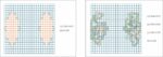
Figure 1 shows that even when the targeted set of incident angles forms two leaf shapes in the pupil plane, corresponding to a certain number of photons for each angle channel, the actual photon distribution among the channels is stochastic, with some channels getting no photons, others getting an excessive number. The absorbed dose here is 8.36 mJ/cm2, corresponding to the 14% absorption of a 60 mJ/cm2 dose by a 30 nm thick resist with an absorption coefficient of 5/um.
Figure 1. Stochastic view of the dipole leaf illumination shape targeted for 30 nm pitch on an 0.33 NA EUV system. 8.36 mJ/cm2 absorbed into a 3 nm x 3 nm area. The source is divided into 152 points, each corresponding to 1/11 of the NA, each channeling 0.055 mJ/cm2 to be absorbed. The plotted numbers are the number of 92 eV EUV photons channeled at the particular incident angle targeting the 3 nm x 3 nm pixel. Left: targeted pupil shape. Right: example of actual distribution of absorbed photons corresponding to each incident angle.
Thus, although the uniform dipole leaf illumination is prescribed for 30 nm line pitch, the actual illumination is effectively a randomly fluctuating subset of this shape, with some angles getting excessive brightness. This results in random image shifts.
Those familiar with using a lithography system may realize that the number of illuminator angle channels affects the degree of fluctuation at a given dose. Hence, reducing the number of channels, or reducing the pupil fill, should be able to alleviate this effect. Through Figures 2 and 3, we get an idea of this improvement.
Figure 2. Stochastic view of the double slot illumination shape targeted for 40 nm pitch on an 0.33 NA EUV system. 10.9 mJ/cm2 absorbed into a 4 nm x 4 nm area. The source is divided into 76 points, each corresponding to 1/11 of the NA, each channeling 0.143 mJ/cm2 to be absorbed. The plotted numbers are the number of 92 eV EUV photons channeled at the particular incident angle targeting the 4 nm x 4 nm pixel. Left: targeted pupil shape. Right: example of actual distribution of absorbed photons corresponding to each incident angle.
Figure 3. Stochastic view of the small dipole illumination shape targeted for 40 nm pitch on an 0.33 NA EUV system. 10.9 mJ/cm2 absorbed into a 4 nm x 4 nm area. The source is divided into 12 points, each corresponding to 1/11 of the NA, each channeling 0.906 mJ/cm2 to be absorbed. The plotted numbers are the number of 92 eV EUV photons channeled at the particular incident angle targeting the 4 nm x 4 nm pixel. Left: targeted pupil shape. Right: example of actual distribution of absorbed photons corresponding to each incident angle.
With the much lower (~3%) pupil fill shown in Figure 3, there is less obvious stochastic distortion of the illumination shape from the target prescription. However, such a low pupil fill means much of the light from the source is cut out by the EUV illuminator itself, forcing the stage to slow down to accumulate the correct dose per unit area. This limits the system throughput severely. While a higher pupil fill had the traditional advantage of imaging a less restricted variety of pitches and shapes, stochastic considerations once again force yet another tradeoff.